|
|
PDF XP1005-BD Data sheet ( Hoja de datos )
| Número de pieza | XP1005-BD | |
| Descripción | Power Amplifier | |
| Fabricantes | MA-COM | |
| Logotipo |  |
|
Hay una vista previa y un enlace de descarga de XP1005-BD (archivo pdf) en la parte inferior de esta página. Total 9 Páginas | ||
|
No Preview Available !
XP1005-BD
Power Amplifier
35.0-43.0 GHz
Features
Excellent Saturated Output Stage
Balanced Design Provides Good Output Match
26.0 dB Small Signal Gain
+24.0 dBm Saturated Output Power
100% On-Wafer RF, DC and Output Power
Testing
100% Commercial-Level Visual Inspection Using
Mil-Std-883 Method 2010
RoHS* Compliant and 260°C Reflow Compatible
Description
M/A-COM Tech’s four stage 35.0-43.0 GHz GaAs
MMIC power amplifier has a small signal gain of
26.0 dB with a +24.0 dBm saturated output power.
The device also includes Lange couplers to achieve
good output return loss. This MMIC uses M/A-COM
Tech’s GaAs PHEMT device model technology, and
is based upon electron beam lithography to ensure
high repeatability and uniformity. The chip has
surface passivation to protect and provide a rugged
part with backside via holes and gold metallization to
allow either a conductive epoxy or eutectic solder
die attach process. This device is well suited for
Millimeter-wave Point-to-Point Radio, LMDS,
SATCOM and VSAT applications.
Ordering Information
Part Number
Package
XP1005-BD-000V
“V” - vacuum release
gel paks
XP1005-BD-EV1
evaluation module
Chip Device Layout
Rev. V2
Absolute Maximum Ratings
Parameter
Absolute Max.
Supply Voltage (Vd)
Supply Current (Id)
Gate Bias Voltage (Vg)
Input Power (Pin)
Storage Temperature (Tstg)
Operating Temperature (Ta)
Channel Temperature (Tch)
+6.0 VDC
1050 mA
+0.3 V
+8.0 dBm
-65 °C to +165 °C
-55 °C to MTTF
Table1
MTTF Table1
1. Channel temperature directly affects a device's MTTF. Chan-
nel temperature should be kept as low as possible to maximize
lifetime.
1
ADVANCED: Data Sheets contain information regarding a product M/A-COM Technology Solutions • North America Tel: 800.366.2266 • Europe Tel: +353.21.244.6400
is considering for development. Performance is based on target specifications, simulated results,
and/or prototype measurements. Commitment to develop is not guaranteed.
PRELIMINARY: Data Sheets contain information regarding a product M/A-COM Technology
• India Tel: +91.80.43537383
• China Tel: +86.21.2407.1588
Visit www.macomtech.com for additional data sheets and product information.
Solutions has under development. Performance is based on engineering tests. Specifications are
typical. Mechanical outline has been fixed. Engineering samples and/or test data may be available. M/A-COM Technology Solutions Inc. and its affiliates reserve the right to make
Commitment to produce in volume is not guaranteed.
changes to the product(s) or information contained herein without notice.
1 page 
XP1005-BD
Power Amplifier
35.0-43.0 GHz
Mechanical Drawing
1.825
(0.072)
1.163
(0.046)
2
1.562
(0.062)
1.960
(0.077)
34
2.362
(0.093)
5
2.764
(0.109)
6
3.162
(0.125)
7
Rev. V2
0.831
(0.033)
1
8
0.478
(0.019)
0.0
0.0
14
1.163
(0.046)
13
1.562
(0.062)
12
1.960
(0.077)
11
2.362
(0.093)
10
2.764
(0.109)
9
3.162 3.526
(0.125) (0.139)
(Note: Engineering designator is 38H4PBA0157)
Units:millimeters (inches) Bond pad dimensions are shown to center of bond pad.
Thickness:0.110 +/- 0.010 (0.0043 +/- 0.0004),Backside is ground,Bond Pad/Backside Metallization:Gold
All DCBond Pads are 0.100 x 0.100 (0.004 x 0.004).All RFBond Pads are 0.100 x 0.200 (0.004 x 0.008)
Bond pad centers are approximately 0.109 (0.004) from the edge of the chip.
Dicing tolerance:+/- 0.005 (+/- 0.0002).Approximate weight:3.987 mg.
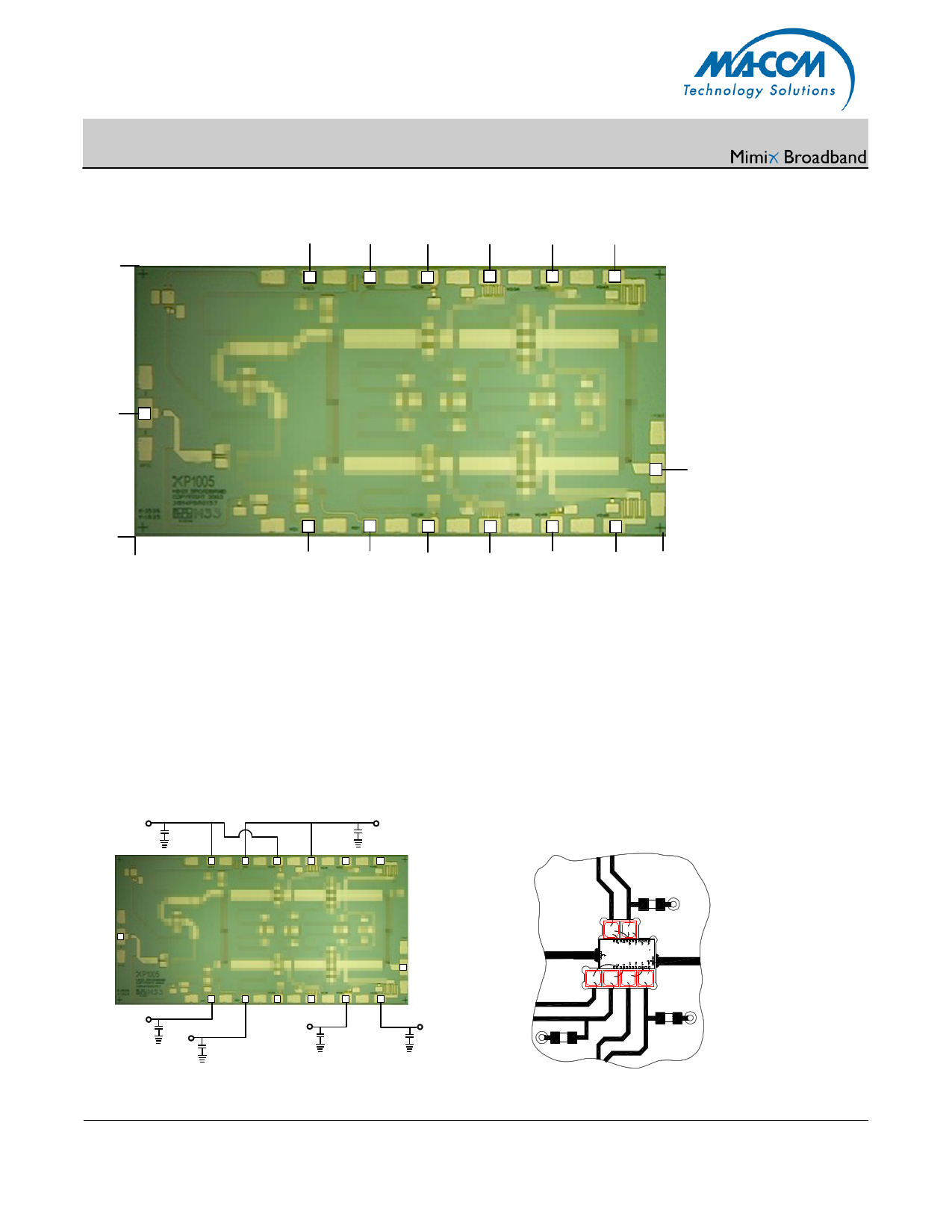
Bond Pad #1 (RFIn)
Bond Pad #2 (Vg2)
Bond Pad #3 (Vd2)
Bond Pad #4 (Vg3A)
Bond Pad #5 (Vd3A)
Bond Pad #6 (Vg4A)
Bond Pad #7 (Vd4A)
Bond Pad #8 (RFOut)
Bond Pad #9 (Vd4B)
Bond Pad #10 (Vg4B)
Bond Pad #11 Vd3B)
Bond Pad #12 (Vg3B)
Bond Pad #13 (Vd1)
Bond Pad #14 (Vg1)
Bias Arrangement
Vg2,3
Vd2,3
2 34 5 6 7
Bypass Capacitors - See App Note [2]
Vg2,3 Vd2,3
RF In 1
Vg1
14
Vd1
13 12
11
Vg4
10
8 RF Out
9
Vd4
RF In
Vg1
Vd1
XP1005-BD
Vg4 Vd4
RF Out
5
ADVANCED: Data Sheets contain information regarding a product M/A-COM Technology Solutions • North America Tel: 800.366.2266 • Europe Tel: +353.21.244.6400
is considering for development. Performance is based on target specifications, simulated results,
and/or prototype measurements. Commitment to develop is not guaranteed.
PRELIMINARY: Data Sheets contain information regarding a product M/A-COM Technology
• India Tel: +91.80.43537383
• China Tel: +86.21.2407.1588
Visit www.macomtech.com for additional data sheets and product information.
Solutions has under development. Performance is based on engineering tests. Specifications are
typical. Mechanical outline has been fixed. Engineering samples and/or test data may be available. M/A-COM Technology Solutions Inc. and its affiliates reserve the right to make
Commitment to produce in volume is not guaranteed.
changes to the product(s) or information contained herein without notice.
5 Page | ||
| Páginas | Total 9 Páginas | |
| PDF Descargar | [ Datasheet XP1005-BD.PDF ] | |
Hoja de datos destacado
| Número de pieza | Descripción | Fabricantes |
| XP1005-BD | Power Amplifier | MA-COM |
| Número de pieza | Descripción | Fabricantes |
| SLA6805M | High Voltage 3 phase Motor Driver IC. |
Sanken |
| SDC1742 | 12- and 14-Bit Hybrid Synchro / Resolver-to-Digital Converters. |
Analog Devices |
|
DataSheet.es es una pagina web que funciona como un repositorio de manuales o hoja de datos de muchos de los productos más populares, |
| DataSheet.es | 2020 | Privacy Policy | Contacto | Buscar |
