|
|
|
PDF NX2139A Data sheet ( Hoja de datos )
| Número de pieza | NX2139A | |
| Descripción | SINGLE CHANNEL MOBILE PWM AND LDO CONTROLLER | |
| Fabricantes | Microsemi | |
| Logotipo | ||
Hay una vista previa y un enlace de descarga de NX2139A (archivo pdf) en la parte inferior de esta página. Total 21 Páginas | ||
|
No Preview Available !
NX2139A
SINGLE CHANNEL MOBILE PWM AND LDO CONTROLLER
PRODUCTION DATA SHEET
DESCRIPTION
The NX2139A controller IC is a compact Buck control-
ler IC with 16 lead MLPQ package designed for step
down DC to DC converter in portable applications. It
can be selected to operate in synchronous mode or
non-synchronous mode to improve the efficiency at light
n
n
n
n
n
load.Constant on time control provides fast response,
good line regulation and nearly constant frequency un-
n
der wide voltage input range. The NX2139 A controller
is optimized to convert single supply up to 22V bus
voltage to as low as 0.75V output voltage. Over cur-
rent protection and FB UVLO followed by latch fea-
ture. A built-in LDO controller can drive an external N-
MOSFET to provide a second output voltage from ei-
ther PWM output source or other power source. Both
PWM controller and LDO controller have separate EN
n
n
n
n
n
n
feature. Other features includes: 5V gate drive capa-
bility, power good indicator, over voltage protection, n
internal Boost schottky diode and adaptive dead band n
control.
n
n
Pb Free Product
FEATURES
Internal Boost Schottky Diode
Ultrasonic mode operation available
Bus voltage operation from 4.5V to 22V
Less than 1uA shutdown current with Enable low
Excellent dynamic response with constant on time
control
Selectable between Synchronous CCM mode and
diode emulation mode to improve efficiency at
light load
Programmable switching frequency
Current limit and FB UVLO with latch off
Over voltage protection with latch off
LDO controller with seperate enable
Two independent Power Good indicator available
Pb-free and RoHS compliant
APPLICATIONS
Notebook PCs and Desknotes
Tablet PCs/Slates
On board DC to DC such as
12V to 3.3V, 2.5V or 1.8V
Hand-held portable instruments
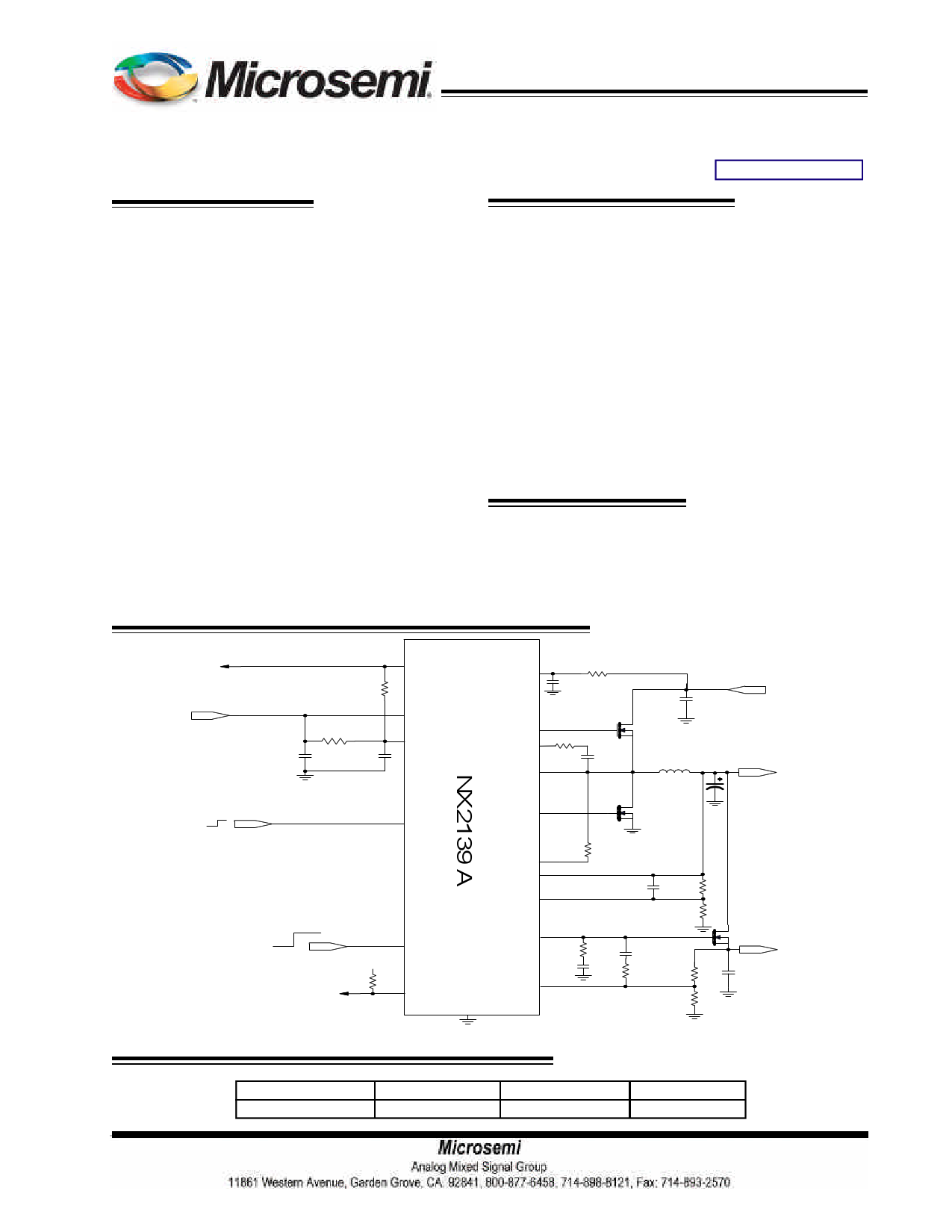
TYPICAL APPLICATION
PGOOD
5V
4 PGOOD
100k
9 PVCC
10 2 VCC
1u 1u
15
ENSW
/MODE
TON 16
1MEG
1n
VIN 7V~22V
2x10uF
HDRV 12
BST 13 2.2
SW 11
IRF7807
1u
1.5uH
LDRV 8
AO4714
Vout 1.8V/7A
2R5TPE330MC
330uF
OCSET 10
5k
VOUT 1
FB 3
330p
10.5k
7.5k
14
ENLDO
LDODRV 7
50
1n
M3
SI4800
1.5V@2A
5V
100k
LDOPG
5 LDOPG
33n
LDOFB 6
GND
PAD
20k
7.5k
7.5k
2x10uF
Figure1 - Typical application of NX2139A
ORDERING INFORMATION
Device
Temperature
Package
NX2139ACMTR -10 o C to 100o C 3X3 MLPQ-16L
Pb-Free
Yes
Rev. 2.4
06/13/12
1
1 page 
NX2139A
PIN DESCRIPTIONS
PIN NUMBER PIN SYMBOL
PIN DESCRIPTION
This pin is directly connected to the output of the switching regulator and
1 VOUT senses the VOUT voltage. An internal MOSFET discharges the output during
turn off.
This pin supplies the internal 5V bias circuit. A 1uF X7R ceramic capacitor is
2
VCC
placed as close as possible to this pin and ground pin.
This pin is the error amplifiers inverting input. This pin is connected via
3 FB resistor divider to the output of the switching regulator to set the output DC
voltage from 0.75V to 3.3 V.
PGOOD indicator for switching regulato r. It requires a pull up resistor to Vcc
4 PGOOD or lower voltage. When FB pin reaches 90% of the reference voltage
PGOOD transitions from LO to HI state.
PGOOD indicator for LDO, requires a pull up resistor to Vcc or lower volt-
5 LDOPG age. When LDOFB pin reaches 90% of the reference voltage PGOOD
transitions from LO to HI state.
This pin is the error amplifiers inverting input. This pin is connected via
6 LDOFB resistor divider to the output of the LDO to set the output DC voltage.
7 LDODRV The drive signal for external LDO N channel MOSFE T.
8 LDRV Low side gate driver output.
9 PVCC Provide the voltage supply to the lower MOSFET drivers. Place a high
frequency decoupling capacitor 1uF X5R to this pin.
10 OCSET This pin is connected to the drain of the external low side MOSFET and is
the input of over current protection(OCP) comparato r. An internal current
source is flown to the external resistor which sets the OCP voltage across
the Rdson of the low side MOSFE T.
11 SW This pin is connected to source of high side FE Ts and provide return path for
the high side driver. It is also the input of zero current sensing comparato r.
12 HDRV High side gate driver output.
This pin supplies voltage to high side FET drive r. A high freq 1uF X7R
13
BST
ceramic capacitor and 2.2ohm resistor in series are recommended to be
placed as close as possible to and connected to this pin and S W pin.
14 ENLDO LDO enable input functions only when ENS W/MODE is not shutdown.
15 ENSW/ Switching converter enable input. Connect to VCC for PFM/Non synchronous
MODE mode, connected to an external resistor divider equals to 70%VCC for ultra-
sonic, connected to GND for shutdown mode, floating or connected to 2V for
the synchronous mode.
16
TON
VIN sensing input. A resistor connects from this pin to VIN will set the fre-
quency. A 1nF capacitor from this pin to GND is recommended to ensure the
proper operation.
PAD
GND Power ground.
Rev. 2.4
06/13/12
5
5 Page 
NX2139A
APPLICATION INFORMATION FS is around 220kHz.
Symbol Used In Application Information:
VIN - Input voltage
VOUT - Output voltage
IOUT - Output current
DVRIPPLE - Output voltage ripple
FS - Working frequency
DIRIPPLE - Inductor current ripple
Output Inductor Selection
The value of inductor is decided by inductor ripple
current and working frequenc y. Larger inductor value
normally means smaller ripple current. However if the
inductance is chosen too large, it brings slow response
and lower efficiency. The ripple current is a design free-
dom which can be decided by design engineer accord-
Design Example
The following is typical application for NX2139A,
the schematic is figure 1.
VIN = 7 to 22V
VOUT=1.8V
FS=220kHz
ing to various application requirements. The inductor
value can be calculated by using the following equa-
tions:
( )LOUT =
VIN -VOUT ON× T
IRIPPLE
IRIPPLE =k × IOUTPUT
...(3)
IOUT=7A
DVRIPPLE <=60mV
DVDROOP<=60mV @ 3A step
On_Time and Frequency Calculation
The constant on time control technique used in
NX2139A delivers high efficienc y, excellent transient
dynamic response, make it a good candidate for step
down notebook applications.
An internal one shot timer turns on the high side
where k is percentage of output current.
In this example, inductor from COILCRAFT
DO5010H-152 with L=1.5uH is chosen.
Current Ripple is recalculated as below:
IRIPPLE
=
(VIN
-VOUT O)N×
LOUT
T
=(22V-1.8V) × 372nS
1.5uH
=5A
...(4)
driver with an on time which is proportional to the input
supply VIN as well inversely proportional to the output Output Capacitor Selection
voltage VOUT. During this time, the output inductor
Output capacitor is basically decided by the
charges the output cap increasing the output voltage amount of the output voltage ripple allowed during
by the amount equal to the output ripple. Once the
steady state(DC) load condition as well as specifica-
timer turns off, the Hdrv turns off and cause the output tion for the load transient. The optimum design may
voltage to decrease until reaching the internal FB volt- require a couple of iterations to satisfy both conditions.
age of 0.75V on the PFM comparator. At this point the Based on DC Load Condition
comparator trips causing the cycle to repeat itself. A
The amount of voltage ripple during the DC load
minimum off time of 400nS is internally set.
condition is determined by equation(5).
The equation setting the On Time is as follows:
TON = 4.45 × 10⁻¹² × RTON × VOUT
VIN − 0.5V
...(1)
FS
=
VOUT
VIN × TON
...(2)
∆VRIPPLE
=
ESR × ∆IRIPPLE
+
∆IRIPPLE
8 × FS × COUT
...(5)
Where ESR is the output capacitors' equivalent
series resistance,C OUT is the value of output capaci-
tors.
Typically POSCAP is recommended to use in
In this application example, the RTON is chosen NX2139's applications. The amount of the output volt-
to be 1Mohm , when VIN=22V, the TON is 372nS and age ripple is dominated by the first term in equation(5)
Rev. 2.4
06/13/12
11
11 Page | ||
| Páginas | Total 21 Páginas | |
| PDF Descargar | [ Datasheet NX2139A.PDF ] | |
Hoja de datos destacado
| Número de pieza | Descripción | Fabricantes |
| NX2139A | SINGLE CHANNEL MOBILE PWM AND LDO CONTROLLER | Microsemi |
| Número de pieza | Descripción | Fabricantes |
| SLA6805M | High Voltage 3 phase Motor Driver IC. |
Sanken |
| SDC1742 | 12- and 14-Bit Hybrid Synchro / Resolver-to-Digital Converters. |
Analog Devices |
|
DataSheet.es es una pagina web que funciona como un repositorio de manuales o hoja de datos de muchos de los productos más populares, |
| DataSheet.es | 2020 | Privacy Policy | Contacto | Buscar |