|
|
|
PDF ADP1290 Data sheet ( Hoja de datos )
| Número de pieza | ADP1290 | |
| Descripción | 2A Logic Controlled High-Side Power Switch | |
| Fabricantes | Analog Devices | |
| Logotipo | ||
Hay una vista previa y un enlace de descarga de ADP1290 (archivo pdf) en la parte inferior de esta página. Total 12 Páginas | ||
|
No Preview Available !
Data Sheet
FEATURES
Low RDSON of 40 mΩ
Wide input voltage range: 2.3 V to 13.2 V
2 A continuous operating current, TJ = <85°C
1.2 V logic compatible enable input
Low 15 µA quiescent current, VIN = 3.3 V
Low 19 µA quiescent current, VIN = 6.5 V
Ultralow shutdown current: 2.0 µA at VIN = 6.5 V
Ultrasmall 1.0 mm × 1.5 mm, 6-ball, 0.5 mm pitch WLCSP
APPLICATIONS
Mobile phones
Digital cameras and audio devices
Portable and battery-powered equipment
GENERAL DESCRIPTION
The ADP1290 is a high-side load switch designed for operation
between 2.3 V and 13.2 V. This load switch provides power
domain isolation, helping to extend battery operation. The
device contains a low on-resistance, N-channel MOSFET that
supports more than 2 A of continuous current and minimizes
power loss. In addition, RDSON is constant independent of the VIN
voltage. The low 15 µA quiescent current and ultralow shutdown
current of 20 µA make the ADP1290 ideal for battery-operated
portable equipment. The built-in level shifter for enable logic
makes the ADP1290 compatible with many processors and
general-purpose input/output (GPIO) controllers.
12 V, 2 A Logic Controlled
High-Side Power Switch
ADP1290
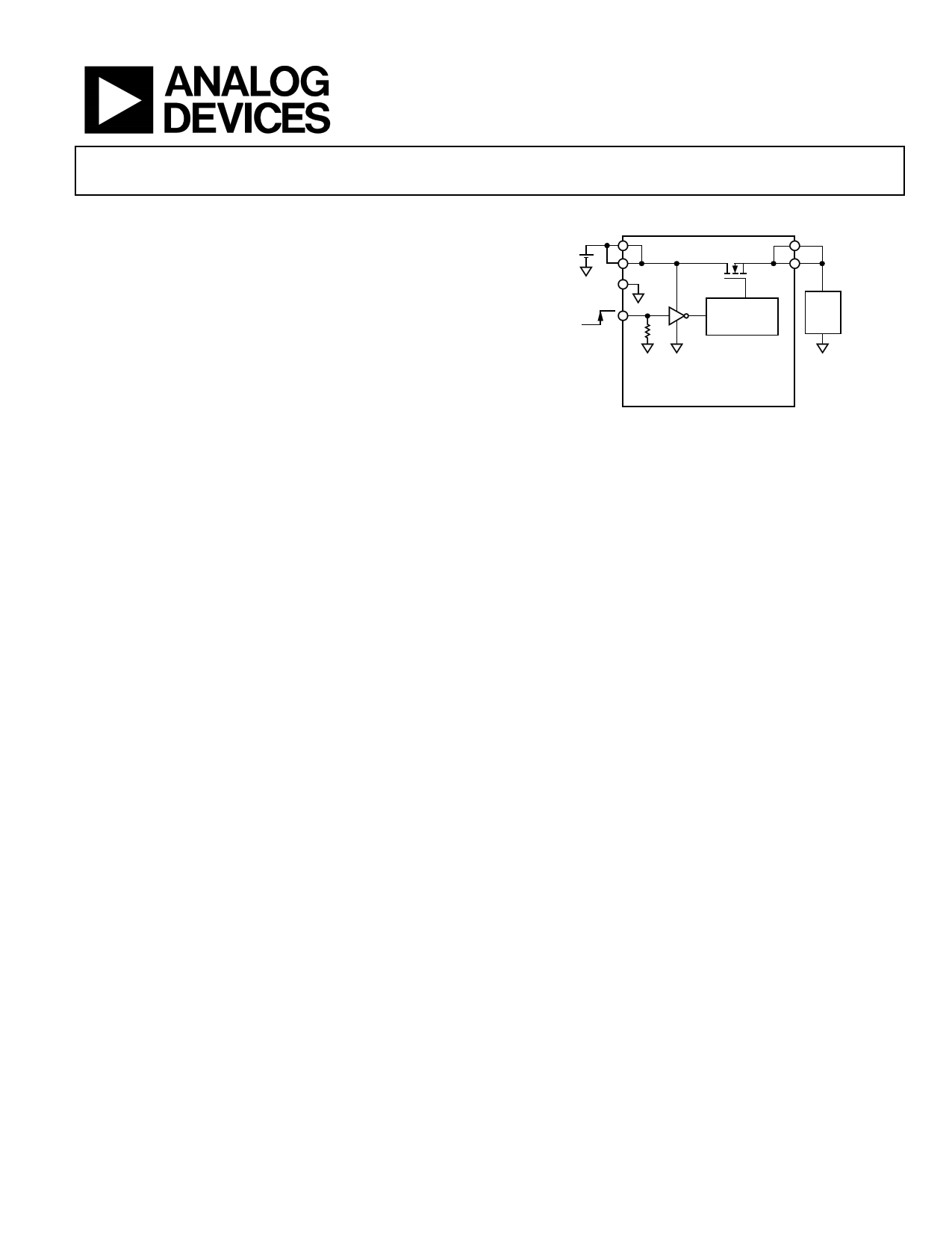
TYPICAL APPLICATIONS CIRCUIT
VIN
+
–
VOUT
GND
ON
EN OFF
CHARGE
PUMP
LOAD
ADP1290
Figure 1.
In addition to operating performance, the ADP1290 occupies
minimal printed circuit board (PCB) space with an area of less
than 1.5 mm2 and a height of 0.60 mm.
The ADP1290 is available in an ultrasmall, 1 mm × 1.5 mm,
6-ball, 0.5 mm pitch WLCSP.
Rev. 0
Document Feedback
Information furnished by Analog Devices is believed to be accurate and reliable. However, no
responsibility is assumed by Analog Devices for its use, nor for any infringements of patents or other
rights of third parties that may result from its use. Specifications subject to change without notice. No
license is granted by implication or otherwise under any patent or patent rights of Analog Devices.
Trademarksandregisteredtrademarksarethepropertyoftheirrespectiveowners.
One Technology Way, P.O. Box 9106, Norwood, MA 02062-9106, U.S.A.
Tel: 781.329.4700
©2014 Analog Devices, Inc. All rights reserved.
Technical Support
www.analog.com
1 page 
Data Sheet
PIN CONFIGURATION AND FUNCTION DESCRIPTIONS
1
A VIN
2
VOUT
ADP1290
B VIN
VOUT
C EN
GND
ADP1290
TOP VIEW
(Not to Scale)
Figure 3. Pin Configuration
Table 4. Pin Function Descriptions
Pin No.
Mnemonic Description
A1, B1
VIN Input Voltage.
A2, B2
VOUT
Output Voltage.
C1 EN Enable Input. Drive the EN pin high to turn on the switch. Drive the EN pin low to turn off the switch.
C2
GND
Ground.
Rev. 0 | Page 5 of 12
5 Page 
Data Sheet
ADP1290
TIMING
Turn on delay is defined as the interval between the time that
VEN exceeds the rising threshold voltage and when VOUT rises to
~10% of its final value. The ADP1290 includes circuitry that has
a typical 250 μs turn on delay and a controlled rise time to limit
the VIN inrush current. As shown in Figure 24 and Figure 25,
the turn on delay is nearly independent of the input voltage.
EN
1
INPUT CURRENT
3
OUTPUT
2
CH1 2.00V BW CH2 2.00V BW M400µs
CH3 100mAΩ BW
T 10.40%
A CH4 1.04V
Figure 24. Typical Turn On Time and Inrush Current, VIN = 2.5 V,
COUT = 10 μF, RLOAD = 100 Ω
Figure 26 and Figure 27 show the typical turn off times with
VIN = 6.5 V, COUT = 10 μF and 100 μF, and RLOAD = 100 Ω.
EN
1
OUTPUT
2
CH1 2.00V BW CH2 2.00V BW M400µs
T 10.40%
A CH4 1.04V
Figure 26. Typical Turn Off Time, COUT = 10 μF, RLOAD = 100 Ω
EN
1
EN
1
INPUT CURRENT
3
OUTPUT
2
CH1 2.00V BW CH2 5.00V BW M400µs
CH3 200mAΩ BW
T 10.40%
A CH4 1.04V
Figure 25. Typical Turn On Time and Inrush Current, VIN = 6.5 V,
COUT = 10 μF, RLOAD = 100 Ω
The rise time is defined as the time it takes the output voltage
to rise from 10% to 90% of VOUT reaching its final value. The turn
on delay is dependent on the rise time of the internal charge pump.
For very large values of output capacitance, the RC time constant
(where C is the load capacitance, CLOAD, and R is the RDSON||RLOAD)
can become a factor in the rise time of the output voltage. Because
RDSON is much smaller than RLOAD, an adequate approximation for
RC is RDSON × CLOAD. An input or load capacitor is not required for
the ADP1290; however, capacitors can suppress noise on the board.
The turn off time is defined as the time it takes for the output
voltage to fall from 90% to 10% of VOUT reaching its final value. The
turn off time is also dependent on the RC time constant of the
output capacitance (CLOAD) and load resistance (RLOAD).
OUTPUT
2
CH1 1.00V BW CH2 2.00V BW M400µs
T 10.40%
A CH4 1.08V
Figure 27. Typical Turn Off Time, COUT = 100 μF, RLOAD = 100 Ω
CURRENT AND THERMAL OVERLOAD
PRECAUTIONS
The ADP1290 is not protected against damage due to excessive
power dissipation and does not have thermal overload protection
circuits. To prevent permanent damage, never allow current
through the ADP1290 to exceed its rated value for more than a
few milliseconds. Permanent damage can also occur if the
output is shorted to ground
THERMAL CONSIDERATIONS
To guarantee reliable operation, the junction temperature of the
ADP1290 must not exceed 105°C. To ensure that the junction
temperature stays below this maximum value, the user must be
aware of the parameters that contribute to junction temperature
changes. These parameters include ambient temperature, power
dissipation in the power device, and thermal resistances between
the junction and ambient air (θJA). The θJA number is dependent
on the package assembly and the amount of copper used to solder
the package pins to the PCB.
Rev. 0 | Page 11 of 12
11 Page | ||
| Páginas | Total 12 Páginas | |
| PDF Descargar | [ Datasheet ADP1290.PDF ] | |
Hoja de datos destacado
| Número de pieza | Descripción | Fabricantes |
| ADP1290 | 2A Logic Controlled High-Side Power Switch | Analog Devices |
| ADP1291 | PRECISION SEMICONDUCTOR PRESSURE SENSOR | ETC |
| Número de pieza | Descripción | Fabricantes |
| SLA6805M | High Voltage 3 phase Motor Driver IC. |
Sanken |
| SDC1742 | 12- and 14-Bit Hybrid Synchro / Resolver-to-Digital Converters. |
Analog Devices |
|
DataSheet.es es una pagina web que funciona como un repositorio de manuales o hoja de datos de muchos de los productos más populares, |
| DataSheet.es | 2020 | Privacy Policy | Contacto | Buscar |