|
|
|
PDF ADF5355 Data sheet ( Hoja de datos )
| Número de pieza | ADF5355 | |
| Descripción | Microwave Wideband Synthesizer | |
| Fabricantes | Analog Devices | |
| Logotipo | ||
Hay una vista previa y un enlace de descarga de ADF5355 (archivo pdf) en la parte inferior de esta página. Total 30 Páginas | ||
|
No Preview Available !
Data Sheet
Microwave Wideband Synthesizer
with Integrated VCO
ADF5355
FEATURES
GENERAL DESCRIPTION
RF output frequency range: 54 MHz to 13,600 MHz
Fractional-N synthesizer and integer-N synthesizer
High resolution 38-bit modulus
Phase frequency detector (PFD) operation to 125 MHz
Reference frequency operation to 600 MHz
Maintains frequency lock over −40°C to +85°C
Low phase noise, voltage controlled oscillator (VCO)
Programmable divide by 1, 2, 4, 8, 16, 32, or 64 output
Analog and digital power supplies: 3.3 V
Charge pump and VCO power supplies: 5 V, typical
Logic compatibility: 1.8 V
Programmable dual modulus prescaler of 4/5 or 8/9
Programmable output power level
RF output mute function
Analog and digital lock detect
Supported in the ADIsimPLL design tool
APPLICATIONS
Wireless infrastructure (W-CDMA, TD-SCDMA,
WiMAX, GSM, PCS, DCS, DECT)
Point to point/point to multipoint microwave links
Satellites/VSATs
Test equipment/instrumentation
Clock generation
The ADF5355 allows implementation of fractional-N or
integer-N phase-locked loop (PLL) frequency synthesizers
when used with an external loop filter and an external reference
frequency. The wideband microwave VCO design permits
frequency operation from 6.8 GHz to 13.6 GHz at one radio
frequency (RF) output. A series of frequency dividers at another
frequency output permits operation from 54 MHz to 6800 MHz.
The ADF5355 has an integrated VCO with a fundamental
output frequency ranging from 3400 MHz to 6800 MHz. In
addition, the VCO frequency is connected to divide by 1, 2, 4, 8,
16, 32, or 64 circuits that allow the user to generate RF output
frequencies as low as 54 MHz. For applications that require
isolation, the RF output stage can be muted. The mute function
is both pin and software controllable.
Control of all on-chip registers is through a simple 3-wire interface.
The ADF5355 operates with analog and digital power supplies
ranging from 3.15 V to 3.45 V, with charge pump and VCO
supplies from 4.75 V to 5.25 V. The ADF5355 also contains
hardware and software power-down modes.
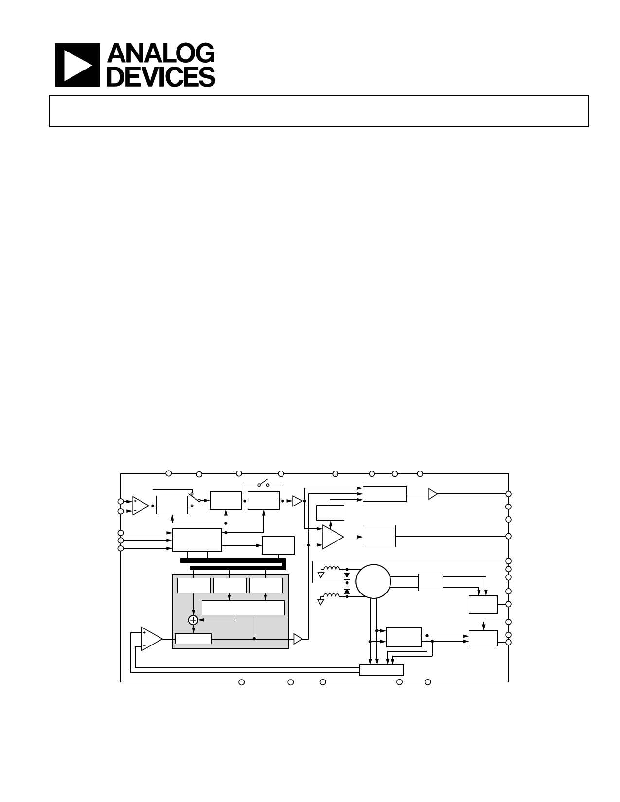
CE AVDD
FUNCTIONAL BLOCK DIAGRAM
AVDD
DVDD
VP RSET VVCO
VRF
REFINA
REFIN B
CLK
DATA
LE
×2
DOUBLER
10-BIT R
COUNTER
÷2
DIVIDER
DATA REGISTER
FUNCTION
LATCH
INTEGER FRACTION MODULUS
REG
REG
REG
THIRD-ORDER
FRACTIONAL INTERPOLATOR
N COUNTER
LOCK
DETECT
MULTIPLEXER
CHARGE
PUMP
PHASE
COMPARATOR
VCO
CORE
×2
÷ 1/2/4/8/
16/32/64
MUXOUT
CREG1
CREG2
CPOUT
OUTPUT
STAGE
OUTPUT
STAGE
VTUNE
VREF
VBIAS
VREGVCO
RFOUTB
PDBRF
RFOUTA+
RFOUTA–
MULTIPLEXER
ADF5355
AGND
CPGND
AGNDRF
Figure 1.
SDGND AGNDVCO
Rev. A
Document Feedback
Information furnished by Analog Devices is believed to be accurate and reliable. However, no
responsibilityisassumedbyAnalogDevices for itsuse,nor foranyinfringementsofpatentsor other
rights of third parties that may result from its use. Specifications subject to change without notice. No
license is granted by implication or otherwise under any patent or patent rights of Analog Devices.
Trademarksandregisteredtrademarksarethepropertyoftheirrespectiveowners.
One Technology Way, P.O. Box 9106, Norwood, MA 02062-9106, U.S.A.
Tel: 781.329.4700 ©2014–2015 Analog Devices, Inc. All rights reserved.
Technical Support
www.analog.com
1 page 
Data Sheet
ADF5355
Parameter
RFOUTA±/RFOUTB Supply Current
Symbol
IRFOUTx±
Low Power Sleep Mode
RF OUTPUT CHARACTERISTICS
VCO Frequency Range
RFOUTB Output Frequency
RFOUTA+/RFOUTA− Output Frequency
VCO Sensitivity
Frequency Pushing (Open-Loop)
Frequency Pulling (Open-Loop)
Harmonic Content
Second
Third
Fundamental VCO Feedthrough
RF Output Power4
KV
RF Output Power Variation
RF Output Power Variation (over Frequency)
Level of Signal with RF Output Disabled
NOISE CHARACTERISTICS
Fundamental VCO Phase Noise Performance
Min
3400
6800
53.125
Typ
16
30
42
55
500
1000
15
15
0.5
30
−27
−22
−20
−12
−8
−55
+8
−3
1
−1
±1
±1
±6
±4
−60
−30
−15
−17
−116
−136
−138
−155
−113
−133
−135
−153
−110
−130
−132
−150
Max
20
35
50
70
6800
13600
6800
Unit Test Conditions/Comments
RFOUTA± output stage is
programmable; enabling RFOUTB
draws negligible extra current
mA −4 dBm setting
mA −1 dBm setting
mA 2 dBm setting
mA 5 dBm setting
µA Hardware power-down selected
µA Software power-down selected
MHz
MHz
MHz
MHz/V
MHz/V
MHz
MHz
Fundamental VCO range
2× VCO output (RFOUTB)
Voltage standing wave ratio (VSWR) =
2:1 RFOUTA+/RFOUTA−
VSWR = 2:1 RFOUTB
dBc
dBc
dBc
dBc
dBm
dBc
dBm
dBm
dBm
dBm
dB
dB
dB
dB
dBm
dBm
dBm
dBm
Fundamental VCO output (RFOUTA+)
Divided VCO output (RFOUTA+)
Fundamental VCO output (RFOUTA+)
Divided VCO output (RFOUTA+)
RFOUTB = 10 GHz
RFOUTA+/RFOUTA− = 1 GHz;
VCO frequency = 4 GHz
RFOUTA+ = 1 GHz; 7.5 nH inductor to VRF
RFOUTA+/RFOUTA− = 6.8 GHz;
7.5 nH inductor to VRF
RFOUTB = 6.8 GHz
RFOUTB = 13.6 GHz
RFOUTA+/RFOUTA− = 5 GHz
RFOUTB = 10 GHz
RFOUTA+/RFOUTA− = 1 GHz to 6.8 GHz
RFOUTB = 6.8 GHz to 13.6 GHz
RFOUTA+/RFOUTA− = 1 GHz
RFOUTA+/RFOUTA− = 6.8 GHz
RFOUTB = 6.8 GHz
RFOUTB = 13.6 GHz
dBc/Hz
dBc/Hz
dBc/Hz
dBc/Hz
dBc/Hz
dBc/Hz
dBc/Hz
dBc/Hz
dBc/Hz
dBc/Hz
dBc/Hz
dBc/Hz
VCO noise in open-loop conditions
100 kHz offset from 3.4 GHz carrier
800 kHz offset from 3.4 GHz carrier
1 MHz offset from 3.4 GHz carrier
10 MHz offset from 3.4 GHz carrier
100 kHz offset from 5.0 GHz carrier
800 kHz offset from 5.0 GHz carrier
1 MHz offset from 5.0 GHz carrier
10 MHz offset from 5.0 GHz carrier
100 kHz offset from 6.8 GHz carrier
800 kHz offset from 6.8 GHz carrier
1 MHz offset from 6.8 GHz carrier
10 MHz offset from 6.8 GHz carrier
Rev. A | Page 5 of 38
5 Page 
Data Sheet
TYPICAL PERFORMANCE CHARACTERISTICS
–50
–70
–90
–110
–130
–150
–170
1k
10k 100k 1M 10M
FREQUENCY OFFSET FROM CARRIER (Hz)
Figure 4. Open-Loop VCO Phase Noise, 3.4 GHz
100M
–50
–70
–90
–110
–130
–150
–170
1k
10k 100k 1M 10M
FREQUENCY OFFSET FROM CARRIER (Hz)
Figure 5. Open-Loop VCO Phase Noise, 5.0 GHz
100M
–50
–70
–90
–110
–130
–150
–170
1k
10k 100k 1M 10M
FREQUENCY OFFSET FROM CARRIER (Hz)
Figure 6. Open-Loop VCO Phase Noise, 6.8 GHz
100M
ADF5355
–50
–70
–90
–110
–130
–150
–170
1k
10k 100k 1M 10M
FREQUENCY OFFSET FROM CARRIER (Hz)
Figure 7. Open-Loop VCO Phase Noise, 8.0 GHz
100M
–50
–70
–90
–110
–130
–150
–170
1k
10k 100k 1M 10M
FREQUENCY OFFSET FROM CARRIER (Hz)
Figure 8. Open-Loop VCO Phase Noise, 10.0 GHz
100M
–50
–70
–90
–110
–130
–150
–170
1k
10k 100k 1M 10M
FREQUENCY OFFSET FROM CARRIER (Hz)
Figure 9. Open-Loop VCO Phase Noise, 13.6 GHz
100M
Rev. A | Page 11 of 38
11 Page | ||
| Páginas | Total 30 Páginas | |
| PDF Descargar | [ Datasheet ADF5355.PDF ] | |
Hoja de datos destacado
| Número de pieza | Descripción | Fabricantes |
| ADF5355 | Microwave Wideband Synthesizer | Analog Devices |
| Número de pieza | Descripción | Fabricantes |
| SLA6805M | High Voltage 3 phase Motor Driver IC. |
Sanken |
| SDC1742 | 12- and 14-Bit Hybrid Synchro / Resolver-to-Digital Converters. |
Analog Devices |
|
DataSheet.es es una pagina web que funciona como un repositorio de manuales o hoja de datos de muchos de los productos más populares, |
| DataSheet.es | 2020 | Privacy Policy | Contacto | Buscar |