|
|
PDF TC62D749CFG Data sheet ( Hoja de datos )
| Número de pieza | TC62D749CFG | |
| Descripción | 16-Output Constant Current LED Driver | |
| Fabricantes | Toshiba | |
| Logotipo |  |
|
Hay una vista previa y un enlace de descarga de TC62D749CFG (archivo pdf) en la parte inferior de esta página. Total 23 Páginas | ||
|
No Preview Available !
TC62D749CFG
TOSHIBA CDMOS Integrated Circuit Silicon Monolithic
TC62D749CFG
16-Output Constant Current LED Driver (Output switching high-speed version)
The TC62D749CFG is a constant-current driver for LED and
LED display lighting applications.
The output current from each of the 16 outputs is
programmable via a single external resistor.
The TC62D749CFG contains a 16-channel shift register, a
16-channel latch, a 16-channel AND gate and a 16-channel
constant-current output.
Fabricated with a CMOS process, the TC62D749CFG allows
high-speed data transfer.
It operates with a 3.3- or 5-V power supply.
SSOP24-P-300-1.00B
Weight: 0.29 g (Typ.)
Features
• Supply voltages
: VDD = 3.0 V to 5.5 V
• 16-output built-in
• Output current setup range
: IOUT = 1.5 to 90 mA
• Constant current output accuracy (@ REXT = 1.2 kΩ, VOUT = 1.0 V, VDD = 3.3 V, 5.0 V)
: S rank;between outputs ± 1.5 % (max)
: S rank;between devices: ± 1.5 % (max)
: N rank;between outputs ± 2.5 % (max)
: N rank;between devices: ± 2.5 % (max)
• Output voltage
: VOUT = 17 V (max)
• High-speed output switching
: twOE = 25 ns (min), tor = 10ns (typ.), tof = 10ns (typ.)
There is TC62D748 as an output switching standard-speed version of this product.
• I/O interface
: CMOS interfaces (Schmitt trigger input)
• Data transfer frequency
: fSCK = 25 MHz (max)
• Operation temperature range
: Topr = −40 to 85 °C
• Power-on-reset function built-in. (When the power supply is turned on, internal data is reset)
• Package
: SSOP24-P-300-1.00B
For detailed part naming conventions, contact your local Toshiba sales representative or distributor.
When the LED driver of high-speed output switching is used, back EMF may occur at the time of output OFF, and
output terminal voltage may rise. Please be careful. It is necessary to reduce inductance to prevent the back EMF. It
is possible to reduce inductance of a substrate by making the power supply for LED wiring shorter and wider
designing the layout pattern.
1 2012-01-10
1 page 
Truth Table
TC62D749CFG
SCK
SLAT
OE
SIN
OUT0 … OUT7 … OUT15 (Note1)
SOUT
H
L
H
− (Note2)
− (Note2)
L
L
L
L
H
Dn
Dn + 1
Dn + 2
Dn + 3
Dn + 3
Dn … Dn − 7 … Dn − 15
No Change
Dn + 2 … Dn − 5 … Dn − 13
Dn + 2 … Dn − 5 … Dn − 13
OFF
Dn − 15
Dn − 14
Dn − 13
Dn − 13
Dn − 13
Note1: When OUT0 to OUT15 output pins are set to "H" the respective output will be ON and when set to
"L" the respective output will be OFF.
Note2: “-“ is irrelevant to the truth table.
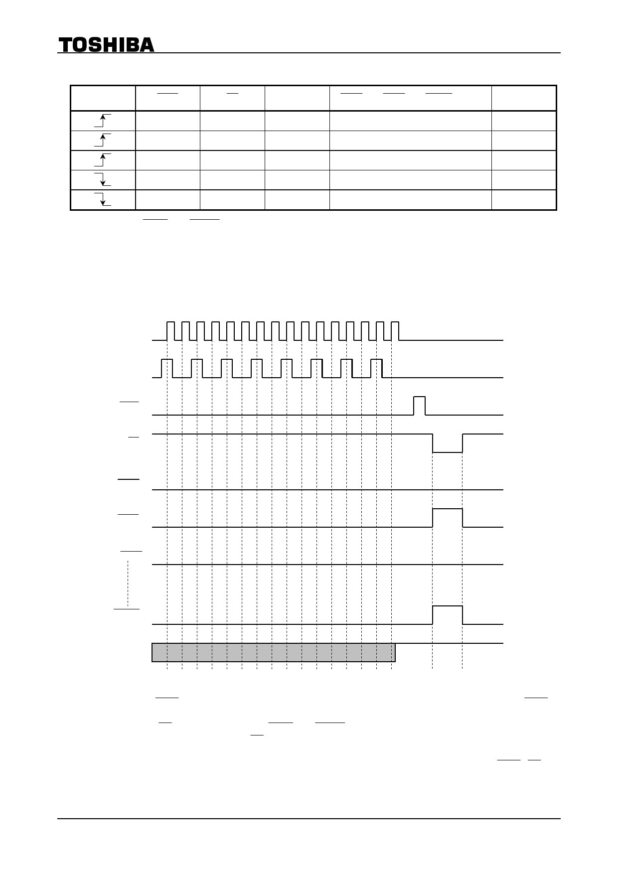
Timing Diagram
SCK
n = 0 1 2 3 4 5 6 7 8 9 10 11 12 13 14 15
SIN
SLAT
OE
OUT0
OUT1
OUT2
H
L
H
L
H
L
H
L
ON
OFF
ON
OFF
ON
OFF
OUT15
SOUT
ON
OFF
H
L
・The latch circuit is a leveled-latch circuit. Please exercise precaution as it is not triggered-latch circuit.
・Keep the SLAT pin is set to “L” to enable the latch circuit to hold data. In addition, when the SLAT
pin is set to “H” the latch circuit does not hold data. The data will instead pass onto output.
When the OE pin is set to “L” the OUT0 to OUT15 output pins will go ON and OFF in response to
the data. In addition, when the OE pin is set to “H” all the output pins will be forced OFF regardless of
the data.
・This product can use 3.3V and 5.0V power supply, but power supply and input (SCK/SIN/ SLAT / OE )
must use same voltage.
5 2012-01-10
5 Page 
Test Circuit4: Power supply current
SCK
F.G SIN
SLAT
OE
VDD
OUT0
OUT7
VIH = VDD
VIL = 0 V
tr = tf = 10 ns
(10 to 90%)
REXT
GND
OUT15
SOUT
TC62D749CFG
A
Test Circuit5: Constant current output / Output OFF leak current / Constant current error
Test Circuit5: Constant current output power supply voltage regulation
Constant current output output voltage regulation
SCK
VDD
OUT0
A
F.G
SIN
SLAT
OE
OUT7
A
VIH = VDD
VIL = 0 V
tr = tf = 10 ns
(10 to 90%)
REXT
GND
OUT15
SOUT
A
Test Circuit6: Switching Characteristics
SCK
F.G SIN
SLAT
OE
VDD
OUT0
OUT7
VIH = VDD
VIL = 0 V
tr = tf = 10 ns
(10 to 90%)
REXT
GND
OUT15
SOUT
RL = 300 Ω
CL
RL
CL
RL
CL = 10.5 pF
11 2012-01-10
11 Page | ||
| Páginas | Total 23 Páginas | |
| PDF Descargar | [ Datasheet TC62D749CFG.PDF ] | |
Hoja de datos destacado
| Número de pieza | Descripción | Fabricantes |
| TC62D749CFG | 16-Output Constant Current LED Driver | Toshiba |
| Número de pieza | Descripción | Fabricantes |
| SLA6805M | High Voltage 3 phase Motor Driver IC. |
Sanken |
| SDC1742 | 12- and 14-Bit Hybrid Synchro / Resolver-to-Digital Converters. |
Analog Devices |
|
DataSheet.es es una pagina web que funciona como un repositorio de manuales o hoja de datos de muchos de los productos más populares, |
| DataSheet.es | 2020 | Privacy Policy | Contacto | Buscar |
