|
|
PDF ISL22102 Data sheet ( Hoja de datos )
| Número de pieza | ISL22102 | |
| Descripción | Dual Audio Logarithmic Potentiometer | |
| Fabricantes | Intersil | |
| Logotipo |  |
|
Hay una vista previa y un enlace de descarga de ISL22102 (archivo pdf) en la parte inferior de esta página. Total 12 Páginas | ||
|
No Preview Available !
ISL22102
Dual, Audio, Push-button Controlled Potentiometer (XDCP™)
Data Sheet
September 21, 2015
FN6788.2
32 Tap, Push-button, Dual Audio
Logarithmic Potentiometer with Buffer
Amplifiers and Audio Detection
The ISL22102 integrates two digitally controlled
potentiometers (DCP) with buffered wiper outputs and an
internal bias voltage generator (VB) on a monolithic CMOS
integrated circuit. The wiper position is adjusted by the user
through simple Up and Down push buttons, ideal for stereo
volume control in audio applications.
Each potentiometer is implemented using 31 polysilicon
resistors in a logarithmic array. Between each of the
resistors are tap points connected to the wiper terminal
through switches. When powered up, the wipers are reset to
the -20dB position.
In addition to the ISL22102’s low noise design, the ISL22102
also contains a zero-crossing detection circuitry to further
minimize click and pop noise during volume transition.
The internal VB generator of the ISL22102 provides a
precision middle scale voltage reference that reduces
external circuitry and simplifies application design.
The ISL22102 implements two power saving techniques for
power critical applications. It is a Standby Mode that can be
enabled to reduce the power consumption of the part when
DCP is not in use. The part also has Audio Detection
circuitry that provides an indication FLAG to external devices
and services. The FLAG can be delayed through D0, D1 and
D2 pin configuration. By connecting the FLAG to the standby
pin (SB), it will automatically put the part into Standby Mode.
Pinout
ISL22102
(20 LD QFN)
TOP VIEW
20 19 18 17 16
DN 1
MUTE 2
VCC 3
AVCC 4
LEFT_IN 5
15 D0
14 VTH
13 GND
12 HPB
11 HPA
6 7 8 9 10
Features
• Dual Audio Control – Two 32 Taps Log Pots
• Buffered Wiper Outputs
• Audio Detection with Threshold Input and Controlled
Delay
• Zero Amplitude Wiper Switching (ZAWS)
• Simple Push-button Interface
• Auto Increment/decrement After 1s Button Press
• Standby Mode
• Mute Function
• Total Resistance: 18.5k each DCP (Typical)
• Voltage Operation
- VCC = 2.7V to 5.5V
- AVCC = 2.7V to 5.5V
• Temp Range = -40°C to +85°C
• Package Options
- 20 Ld TSSOP
- 20 Ld QFN
• Pb-Free (RoHS Compliant)
Audio Performance
• 0dB to -72dB Volume Control
• -90dB Mute
• SNR: -90dB
• THD+N: 0.01% @ 1kHz
• Crosstalk Rejection: -100dB @ 1kHz
• Channel-to-Channel Variation: ±0.1dB
• Mid point 3dB-Cutoff: 100kHz
Applications
• Set Top Boxes
• Stereo Amplifiers
• DVD Players
• Portable Audio Products
1
CAUTION: These devices are sensitive to electrostatic discharge; follow proper IC Handling Procedures.
1-888-INTERSIL or 1-888-468-3774 | Intersil (and design) is a registered trademark of Intersil Americas LLC
XDCP is a trademark of Intersil Americas Inc. Copyright Intersil Americas LLC 2008, 2010, 2015. All Rights Reserved
All other trademarks mentioned are the property of their respective owners.
1 page 
ISL22102
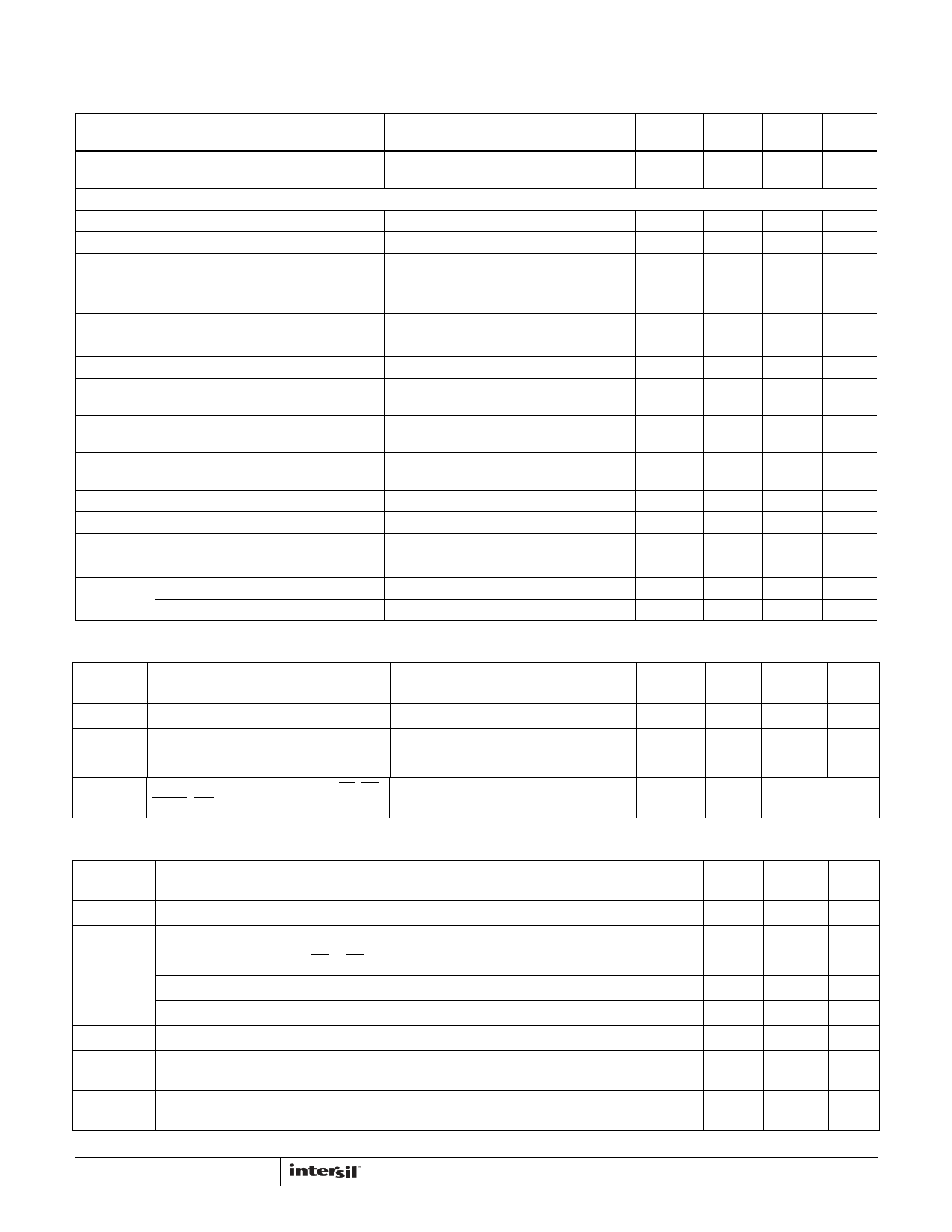
Analog Specifications Over the recommended operating conditions unless otherwise specified.
SYMBOL
PARAMETER
TEST CONDITIONS
TCR Temperature Coefficient of End-to-end
(Note 7) Resistance
DC ELECTRICAL SPECIFICATION
AVCC Analog Power Supply
VCC
Digital Power Supply
tR
IAVCC
AVCC and VCC Ramp Rate
Analog Supply Current
AVCC = 5.5V, IBIAS = 0mA, IOUT = 0mA for
both channels
IASB Analog Standby Current
AVCC = 5.5V, IBIAS = 0mA
ICC1
VCC Supply Current
All Inputs = 5.5V, VCC = 5.5V, AVCC = 5.5V
ISB VCC Current (Standby)
VCC = 5.5V
VIN Input Signal on LEFT_IN, RIGHT_IN Reference to VB pin
Pins
VOUT
Output Signal on LEFT_OUT,
RIGHT_OUT Pins
Reference to GND
IOUT
LEFT_OUT, RIGHT_OUT Buffer Current VCC = 5.5V
(Note 5)
ROUT
CIN (Note 7)
VB
Buffer Output Impedance
Input Capacitance LEFT_IN, RIGHT_IN
Bias Output Voltage
VB Accuracy
IBIAS
VB Output Current
VB Output Impedance
VCC = 5.5V
MIN
(Note 8)
2.7
2.7
0.2
-AVCC/2
0
-15
-50
-5
TYP
(Note 4)
±340
MAX
(Note 8)
UNIT
ppm/°C
5.5 V
5.5 V
50 V/ms
750 µA
360
60
35
AVCC/2
µA
µA
µA
V
AVCC
V
15 mA
10
AVCC/2
25
50
5
20
pF
V
mV
mA
Digital Specifications Over the recommended operating conditions unless otherwise specified.
SYMBOL
PARAMETER
TEST CONDITIONS
MIN TYP MAX
(Note 8) (Note 4) (Note 8) UNITS
ILkg Input Leakage Current
For D0, D1, and D2
VIH Input HIGH Voltage
VIL Input LOW Voltage
Ics Internal Pull-up Current Source on UP, DN,
(Notes 6, 7) MUTE, SB Pins
-0.3 0.3 µA
VCC x 0.7
V
VCC x 0.1 V
1.5 2.75 µA
AC Timing Over recommended operating conditions
SYMBOL
PARAMETER
tPU (Note 7)
tWRPO
(Note 7)
Power-up Time to Wiper Stable
Wiper Response Time (include tDB and tZAWS )
Auto Increment Starts after UP or DN Input is Keeping Low
Auto Increment Rate for the First 4s
Auto Increment Rate After 4s
tDB
tLOCK
(Note 7)
Debounce Time
Lockout Time after Debounce Time, when any New Command will be Ignored
tFLAG_HIGH FLAG Delay Time from when Audio Input is Detected to FLAG Asserted HIGH
(Note 7)
MIN
(Note 8)
TYP MAX
(Note 4) (Note 8)
10
35
1
4
8
50
40
UNITS
ms
ms
s
Hz
Hz
ms
ms
1 µs
5 FN6788.2
September 21, 2015
5 Page 
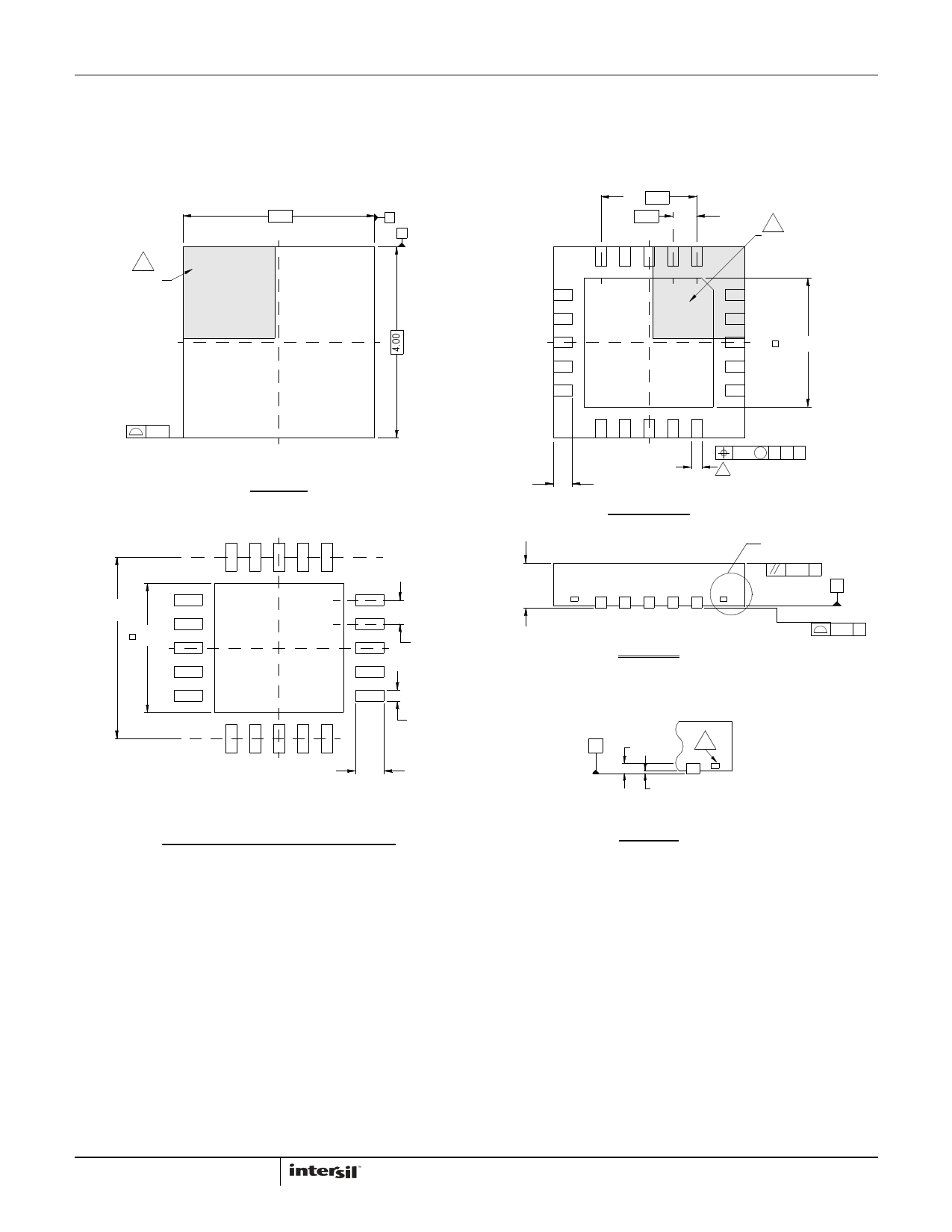
Package Outline Drawing
L20.4x4C
20 LEAD QUAD FLAT NO-LEAD PLASTIC PACKAGE
Rev 0, 11/06
ISL22102
6
PIN 1
INDEX AREA
4.00
A
B
15
4X 2.0
16X 0.50
16
6
20 PIN #1 INDEX AREA
1
(4X) 0.15
TOP VIEW
( 3. 8 TYP )
( 2. 70 )
11
0 . 90 ± 0 . 1
( 20X 0 . 5 )
2 .70 ± 0 . 15
5
10
20X 0.4 ± 0.10
6
0.10 M C A B
4 20X 0.25 +0.05 / -0.07
BOTTOM VIEW
SIDE VIEW
SEE DETAIL "X"
0.10 C
C
BASE PLANE
SEATING PLANE
0.08 C
( 20X 0 . 25 )
( 20X 0 . 6)
TYPICAL RECOMMENDED LAND PATTERN
C
0 . 2 REF
5
0 . 00 MIN.
0 . 05 MAX.
DETAIL "X"
NOTES:
1. Dimensions are in millimeters.
Dimensions in ( ) for Reference Only.
2. Dimensioning and tolerancing conform to AMSE Y14.5m-1994.
3. Unless otherwise specified, tolerance : Decimal ± 0.05
4. Dimension b applies to the metallized terminal and is measured
between 0.15mm and 0.30mm from the terminal tip.
5. Tiebar shown (if present) is a non-functional feature.
6. The configuration of the pin #1 identifier is optional, but must be
located within the zone indicated. The pin #1 indentifier may be
either a mold or mark feature.
11 FN6788.2
September 21, 2015
11 Page | ||
| Páginas | Total 12 Páginas | |
| PDF Descargar | [ Datasheet ISL22102.PDF ] | |
Hoja de datos destacado
| Número de pieza | Descripción | Fabricantes |
| ISL22102 | Dual Audio Logarithmic Potentiometer | Intersil |
| Número de pieza | Descripción | Fabricantes |
| SLA6805M | High Voltage 3 phase Motor Driver IC. |
Sanken |
| SDC1742 | 12- and 14-Bit Hybrid Synchro / Resolver-to-Digital Converters. |
Analog Devices |
|
DataSheet.es es una pagina web que funciona como un repositorio de manuales o hoja de datos de muchos de los productos más populares, |
| DataSheet.es | 2020 | Privacy Policy | Contacto | Buscar |
