|
|
|
PDF NB3V1106C Data sheet ( Hoja de datos )
| Número de pieza | NB3V1106C | |
| Descripción | 3.3V/2.5V/1.8V LVCMOS Low Skew Fanout Buffer Family | |
| Fabricantes | ON Semiconductor | |
| Logotipo | ||
Hay una vista previa y un enlace de descarga de NB3V1106C (archivo pdf) en la parte inferior de esta página. Total 12 Páginas | ||
|
No Preview Available !
NB3V110xC Series
3.3V/2.5V/1.8V LVCMOS
Low Skew Fanout Buffer
Family
Description
The NB3V110xC are a modular, high−performance, low−skew,
general purpose LVCMOS clock buffer family. The family of devices
is designed with a modular approach. Four different fan−out
variations, 1:2, 1:3, 1:4, 1:6 and 1:8, are available. All of the devices
are pin compatible to each other for easy handling. All family
members share the same high performing characteristics like low
additive jitter, low skew, and wide operating temperature range. The
NB3V110xC supports an asynchronous output enable control (OE)
which switches the outputs into a low state when OE is low. The
NB3V110xC devices operate in a 3.3 V, 2.5 V and 1.8 V environment
and are characterized for operation from −40°C to 105°C.
Features
• Operating Temperature Range: –40°C to 105°C
• High−Performance 1:2, 1:3, 1:4, 1:6, 1:8 LVCMOS Clock Buffer
• Available in 8−, 14−, 16−Pin TSSOP and WDFN8 Packages
• Very Low Output−to−Output Skew < 50 ps
• Very Low Additive Jitter < 200 fs
• Supply Voltage: 3.3 V, 2.5 V or 1.8 V
• fmax = 250 MHz for 3.3 V; fmax = 180 MHz for 2.5 V;
fmax = 133 MHz for 1.8 V
• These Devices are Pb−Free and are RoHS Compliant
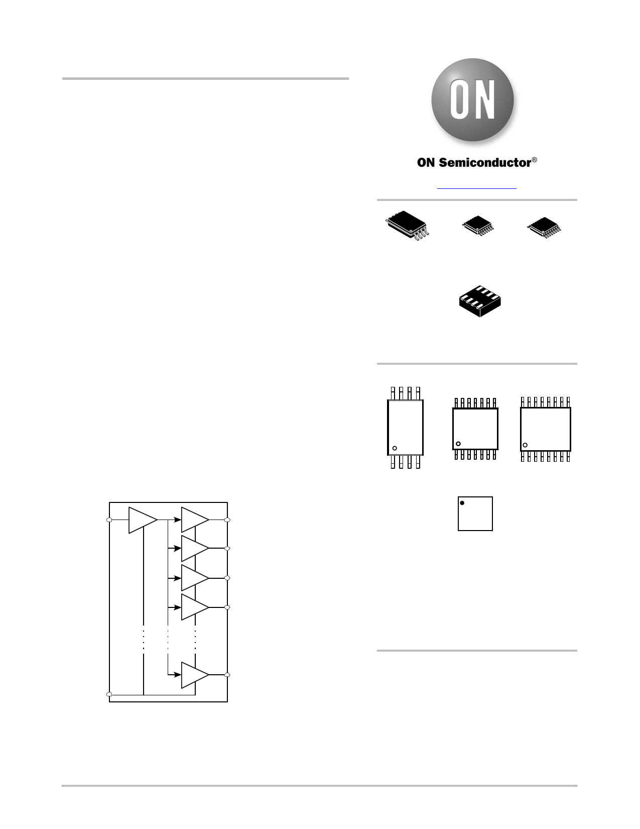
BLOCK DIAGRAM
CLKIN
LV
CMOS
LV
CMOS
Q0
LV
CMOS
Q1
LV
CMOS
Q2
LV
CMOS
Q3
S
S
S
LV
CMOS
Qn
OE
This document contains information on some products that are still under development.
ON Semiconductor reserves the right to change or discontinue these products without
notice.
www.onsemi.com
TSSOP−8
DT SUFFIX
CASE 948S
TSSOP−14
DT SUFFIX
CASE 948G
TSSOP−16
DT SUFFIX
CASE 948F
WDFN8, 2x2
MT SUFFIX
CASE 511AQ
MARKING DIAGRAMS
8
10x
YWW
AG
1
14
1106
V
ALYWG
G
1
16
1108
V
ALYWG
G
1
TSSOP−8
TSSOP−14
TSSOP−16
1
0X MG
G
WDFN8
A = Assembly Location
M = Date Code
L = Wafer Lot
Y = Year
W, WW = Work Week
G = Pb−Free Package
(Note: Microdot may be in either location)
ORDERING INFORMATION
See detailed ordering, marking and shipping information on
page 8 of this data sheet.
© Semiconductor Components Industries, LLC, 2016
March, 2016 − Rev. 2
1
Publication Order Number:
NB3V1102C/D
1 page 
NB3V110xC Series
Table 6. DEVICE CHARACTERISTICS (continued)
Over recommended operating free−air temperature range (unless otherwise noted) (Note 4)
Symbol
Parameter
Condition
Min Typ Max Unit
OUTPUT PARAMETERS FOR VDD = 2.5 V + 0.2 V
VOH High−level output voltage
VDD = 2.3 V, IOH = –0.1 mA
VDD = 2.3 V, IOH = –8 mA
VOL Low−level output voltage
VDD = 2.3 V, IOL = 0.1 mA
VDD = 2.3 V, IOL = 8 mA
tPLH, tPHL Propagation delay (Note 9)
CLKIN to Qn
tsk(o) Output skew (Note 9)
Equal load of each output 85°C
Equal load of each output 105°C
2.2 V
1.7
0.1 V
0.5
1.8 ns
50 ps
60
tr/tf
tDIS
tEN
tsk(p)
Rise and fall time
Output disable time (Note 9)
Output enable time (Note 9)
Pulse skew ; tPLH(Qn) – tPHL(Qn)
(Note 8)
20%–80% (VOH − VOL)
OE to Qn
OE to Qn
To be measured with input duty cycle of 50%
0.2
1.2 ns
10 ns
10 ns
220 ps
tsk(pp) Part−to−part skew
Under equal operating conditions for two
parts
1.2 ns
tjit(f) Additive jitter rms
12 kHz...20 MHz fOUT = 100 MHz
12 kHz...20 MHz fOUT = 156.25 MHz
OUTPUT PARAMETERS FOR VDD = 1.8 V + 5%
VOH High−level output voltage
VDD = 1.71 V, IOH = –0.1 mA
1.6
VDD = 1.71 V, IOH = –4 mA
0.75xVDD
VOL Low−level output voltage
VDD = 1.71 V, IOL = 0.1 mA
VDD = 1.71 V, IOL = 4 mA
tPLH, tPHL Propagation delay (Note 9)
CLKIN to Qn
1.8
tsk(o) Output skew (Note 9)
Equal load of each output
tr/tf Rise and fall time
20%–80% (VOH − VOL)
0.17
tDIS Output disable time (Note 9)
OE to Qn
tEN Output enable time (Note 9)
OE to Qn
tsk(p)
Pulse skew ; tPLH(Qn) – tPHL(Qn)
(Note 8)
To be measured with input duty cycle of 50%
150 fs
100
V
0.1
0.25xVDD
3.5
75
1.2
10
10
450
V
ns
ps
ns
ns
ns
ps
tsk(pp) Part−to−part skew
Under equal operating conditions for two
parts
1.2 ns
tjit(f) Additive jitter rms
12 kHz...20 MHz, fOUT = 100 MHz
200 fs
Product parametric performance is indicated in the Electrical Characteristics for the listed test conditions, unless otherwise noted. Product
performance may not be indicated by the Electrical Characteristics if operated under different conditions.
8. tsk(p) depends on output rise− and fall−time (tr/tf). The output duty−cycle can be calculated: odc = (tw(OUT) ± tsk(p))/tperiod; tw(OUT) is
pulse−width of ideal output waveform and tperiod is 1/fOUT.
9. With rail to rail input clock.
www.onsemi.com
5
5 Page 
NB3V110xC Series
PACKAGE DIMENSIONS
TSSOP−16
CASE 948F
ISSUE B
0.15 (0.006) T U S
16
2X L/2
L
PIN 1
IDENT.
1
0.15 (0.006) T U S
0.10 (0.004)
−T− SEATING
PLANE
D
C
16X K REF
0.10 (0.004) M T U S V S
9 J1
B
−U− J
N
8
K
K1
ÇÇÇÉÉÇÇÇÉÉÇÇÇÉÉSECTION N−N
0.25 (0.010)
M
NOTES:
1. DIMENSIONING AND TOLERANCING PER
ANSI Y14.5M, 1982.
2. CONTROLLING DIMENSION: MILLIMETER.
3. DIMENSION A DOES NOT INCLUDE MOLD
FLASH. PROTRUSIONS OR GATE BURRS.
MOLD FLASH OR GATE BURRS SHALL NOT
EXCEED 0.15 (0.006) PER SIDE.
4. DIMENSION B DOES NOT INCLUDE
INTERLEAD FLASH OR PROTRUSION.
INTERLEAD FLASH OR PROTRUSION SHALL
NOT EXCEED 0.25 (0.010) PER SIDE.
5. DIMENSION K DOES NOT INCLUDE DAMBAR
PROTRUSION. ALLOWABLE DAMBAR
PROTRUSION SHALL BE 0.08 (0.003) TOTAL
IN EXCESS OF THE K DIMENSION AT
MAXIMUM MATERIAL CONDITION.
6. TERMINAL NUMBERS ARE SHOWN FOR
REFERENCE ONLY.
7. DIMENSION A AND B ARE TO BE
DETERMINED AT DATUM PLANE −W−.
A
−V−
G
N
F
DETAIL E
H DETAIL E
−W−
MILLIMETERS INCHES
DIM MIN MAX MIN MAX
A 4.90 5.10 0.193 0.200
B 4.30 4.50 0.169 0.177
C −−− 1.20 −−− 0.047
D 0.05 0.15 0.002 0.006
F 0.50 0.75 0.020 0.030
G 0.65 BSC
0.026 BSC
H 0.18 0.28 0.007 0.011
J 0.09 0.20 0.004 0.008
J1 0.09 0.16 0.004 0.006
K 0.19 0.30 0.007 0.012
K1 0.19 0.25 0.007 0.010
L 6.40 BSC
0.252 BSC
M 0_ 8_ 0_ 8_
SOLDERING FOOTPRINT
7.06
1
16X
0.36
16X
1.26
0.65
PITCH
DIMENSIONS: MILLIMETERS
www.onsemi.com
11
11 Page | ||
| Páginas | Total 12 Páginas | |
| PDF Descargar | [ Datasheet NB3V1106C.PDF ] | |
Hoja de datos destacado
| Número de pieza | Descripción | Fabricantes |
| NB3V1106C | 3.3V/2.5V/1.8V LVCMOS Low Skew Fanout Buffer Family | ON Semiconductor |
| Número de pieza | Descripción | Fabricantes |
| SLA6805M | High Voltage 3 phase Motor Driver IC. |
Sanken |
| SDC1742 | 12- and 14-Bit Hybrid Synchro / Resolver-to-Digital Converters. |
Analog Devices |
|
DataSheet.es es una pagina web que funciona como un repositorio de manuales o hoja de datos de muchos de los productos más populares, |
| DataSheet.es | 2020 | Privacy Policy | Contacto | Buscar |