|
|
|
PDF NB3N3010B Data sheet ( Hoja de datos )
| Número de pieza | NB3N3010B | |
| Descripción | 12.288 MHz Audio Oversampling Clock Generator | |
| Fabricantes | ON Semiconductor | |
| Logotipo | ||
Hay una vista previa y un enlace de descarga de NB3N3010B (archivo pdf) en la parte inferior de esta página. Total 9 Páginas | ||
|
No Preview Available !
NB3N3010B
3.3V, 12.288 MHz Audio
Oversampling Clock
Generator for USB
Applications
Description
The NB3N3010B is a precision, low noise clock multiplier that
generates an output frequency of 12.288 MHz. This is accomplished
by using Frequency−Locked−Loop (FLL) techniques where a 4 kHz
reference input is multiplied by 3072, or an 8 kHz input by 1536. The
frequency multiplier is selected by the S0 pin.
The two LVCMOS output drivers are disabled to a logic Low with
the ENABLEn pin set HIGH. The NB3N3010B operates from a single
+3.3 V supply, and is available in the SOIC−8 pin package, and
optionally in a DFN8 package. The operating temperature range is
from 0°C to +85°C.
The NB3N3010B device provides the optimum combination of low
cost, flexibility, and high performance. This makes it ideal for
applications such as oversampling A−to−D and D−to−A converters
from a low reference frequency, such as a USB start−of−frame (SOF)
pulse.
http://onsemi.com
8
1
SOIC−8
D SUFFIX
CASE 751
MARKING
DIAGRAMS*
8
3010B
ALYW
G
1
DFN8
MN SUFFIX
CASE 506AA
14
Features
• Accepts 8 kHz or 4 kHz Reference Input Derived from USB
Start−of−Frame
• Generates 12.288 MHz Frequency−Locked to the Reference
• Fully Integrated Frequency−Lock−Loop with Internal Loop Filter
• Low Skew Dual LVCMOS Outputs
• Very Low Phase Noise Preserves Codec Noise Floor
• Internal Voltage Regulator
• Supply Voltage Required: +3.3 V $5%
• Temperature Range: 0°C to +85°C
• These are Pb−Free Devices
A = Assembly Location
L = Wafer Lot
Y = Year
W = Work Week
M = Date Code
G = Pb−Free Package
(Note: Microdot may be in either location)
*For additional marking information, refer to
Application Note AND8002/D.
ORDERING INFORMATION
See detailed ordering and shipping information in the package
dimensions section on page 7 of this data sheet.
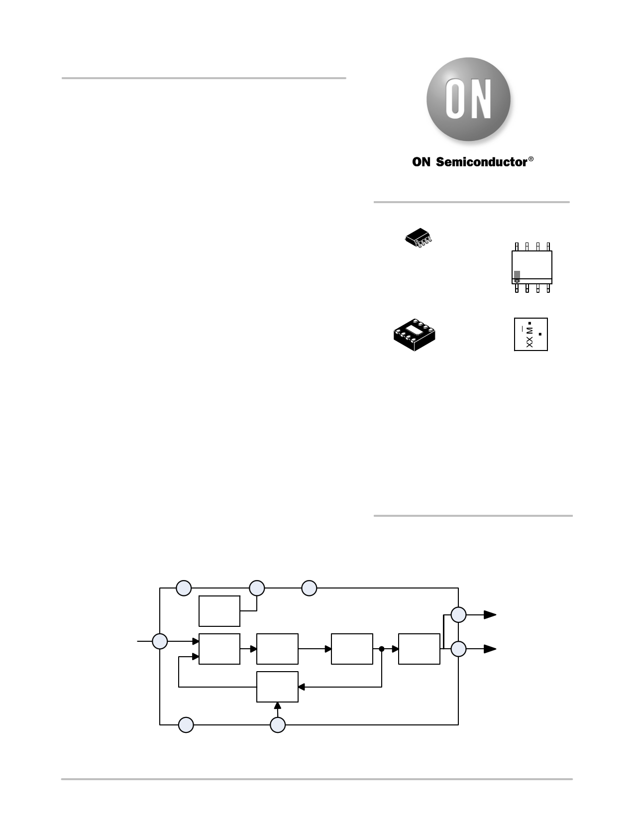
REF
3
VDD
8
+1.8 V
Linear
Regulator
Tolerant
Frequency
Detector
CFILT
5
GND
4
Loop Filter
Frequency
Generator
Output
Buffers
CLK_A
6
CLK_B
7
Divider
1
ENABLEn
2
S0
Figure 1. NB3N3010B Simplified Diagram
© Semiconductor Components Industries, LLC, 2011
May, 2011 − Rev. 0
1
Publication Order Number:
NB3N3010B/D
1 page 
NB3N3010B
APPLICATION INFORMATION
Figure 1 shows the simplified block diagram of the
NB3N3010B device.
The primary function of the NB3N3010B is to accept a
selectable 4 kHz or 8 kHz input reference clock, REF, and
then multiply it to 12.288 MHz output frequency.
Frequency Select − SO
Either of two expected input REF frequencies, 4 kHz or
8 kHz, will be multiplied by the FLL to achieve 12.288 MHz
at the low−skew CLKA and CLKB outputs by selecting the
S0 pin; see Table 6.
The pulse high time (THI) of the input reference signal may
vary widely depending on the application. See AC
specifications for details.
Output Enable − ENABLEn
A Low active output enable input pin, ENABLEn, is
provided. When the ENABLEn input is High inactive, both
clock outputs are driven to a logic Low.
The NB3N3010B implements a delay, specified as
ENABLEn to Output Delay in the AC Specifications, from
the assertion of ENABLEn to the first rising edges on the
clock outputs. This delay insures that CLKA and CLKB
output pulses are within specification before the output
drivers are enabled. When ENABLEn transitions from Low
to High (de−asserts), the current cycle of the clock outputs
completes normally then the outputs will be held Low. The
ENABLEn signal is asynchronous to either the REF input or
CLK_x outputs.
Table 6. INPUT FREQUENCY SELECT AND OUTPUT ENABLE FUNCTIONS
ENABLEn*
0
S0*
L
fREF
4 kHz
FLL Multiplier
3072
CLKA & CLKB Frequency
12.288 MHz
0 H 8 kHz
1536
12.288 MHz
1 xx
x
Disabled Low
*Defaults High when left open.
Typical Power On Sequence
1. Power On
2. Reference Clock present; must be switching before ENABLEn goes High.
3. Output Enable, ENABLEn, High−to−Low
VDD Valid
VDD Valid to ENABLEn
VDD
ENABLEn
Outputs Enabled
4 kHz or
8 kHz
REF
12.288 MHz CLKA/B
400 Clock Cycles @ 8 kHz
200 Clock Cycles @ 4 kHz
ENABLEn to Output
~50 ms, typ
Figure 3. ENABLEn Timing Diagram
Completed Clock
Outputs
Then Low
http://onsemi.com
5
5 Page | ||
| Páginas | Total 9 Páginas | |
| PDF Descargar | [ Datasheet NB3N3010B.PDF ] | |
Hoja de datos destacado
| Número de pieza | Descripción | Fabricantes |
| NB3N3010B | 12.288 MHz Audio Oversampling Clock Generator | ON Semiconductor |
| Número de pieza | Descripción | Fabricantes |
| SLA6805M | High Voltage 3 phase Motor Driver IC. |
Sanken |
| SDC1742 | 12- and 14-Bit Hybrid Synchro / Resolver-to-Digital Converters. |
Analog Devices |
|
DataSheet.es es una pagina web que funciona como un repositorio de manuales o hoja de datos de muchos de los productos más populares, |
| DataSheet.es | 2020 | Privacy Policy | Contacto | Buscar |