|
|
|
PDF LTM4609 Data sheet ( Hoja de datos )
| Número de pieza | LTM4609 | |
| Descripción | High Efficiency Buck-Boost DC/DC uModule Regulator | |
| Fabricantes | Linear Technology | |
| Logotipo | ||
Hay una vista previa y un enlace de descarga de LTM4609 (archivo pdf) en la parte inferior de esta página. Total 28 Páginas | ||
|
No Preview Available !
LTM4609
36VIN, 34VOUT High Efficiency
Buck-Boost DC/DC
µModule Regulator
Features
Description
n Single Inductor Architecture Allows VIN Above,
Below or Equal to VOUT
n Wide VIN Range: 4.5V to 36V
n Wide VOUT Range: 0.8V to 34V
n IOUT: 4A DC (10A DC in Buck Mode)
n Up to 98% Efficiency
n Current Mode Control
n Power Good Output Signal
n Phase-Lockable Fixed Frequency: 200kHz to 400kHz
n Ultrafast Transient Response
n Current Foldback Protection
n Output Overvoltage Protection
n Small Surface Mount Footprint, Low Profile
(15mm × 15mm × 2.82mm) LGA and
(15mm × 15mm × 3.42mm) BGA Packages
n SnPb (BGA) or RoHS Compliant (LGA and BGA)
Finish
Applications
n Telecom, Servers and Networking Equipment
n Industrial and Automotive Equipment
n High Power Battery-Operated Devices
The LTM®4609 is a high efficiency switching mode buck-
boost power supply. Included in the package are the
switching controller, power FETs and support components.
Operating over an input voltage range of 4.5V to 36V, the
LTM4609 supports an output voltage range of 0.8V to
34V, set by a resistor. This high efficiency design delivers
up to 4A continuous current in boost mode (10A in buck
mode). Only the inductor, sense resistor, bulk input and
output capacitors are needed to finish the design.
The low profile package enables utilization of unused space
on the bottom of PC boards for high density point of load
regulation. The high switching frequency and current
mode architecture enable a very fast transient response
to line and load changes without sacrificing stability. The
LTM4609 can be frequency synchronized with an external
clock to reduce undesirable frequency harmonics.
Fault protection features include overvoltage and foldback
current protection. The DC/DC µModule® regulator is of-
fered in small 15mm × 15mm × 2.82mm LGA and 15mm
× 15mm × 3.42mm BGA packages. The LTM4609 is avail-
able with SnPb (BGA) or RoHS compliant terminal finish.
L, LT, LTC, LTM, Linear Technology, the Linear logo, µModule, Burst Mode and PolyPhase are
registered trademarks and No RSENSE is a trademark of Linear Technology Corporation. All other
trademarks are the property of their respective owners.
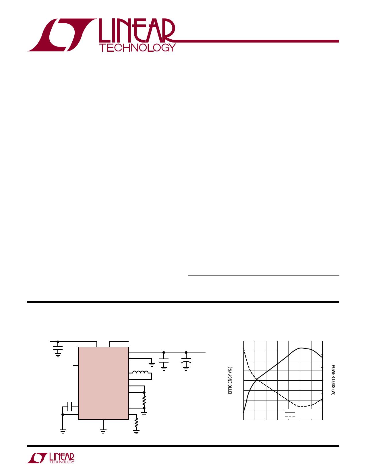
Typical Application
30V/2A Buck-Boost DC/DC µModule Regulator with 6.5V to 36V Input
VIN
6.5V TO 36V
10µF
50V
ON/OFF
0.1µF
CLOCK SYNC
VIN PLLIN VOUT
FCB
RUN LTM4609
SW1
SW2
RSENSE
SENSE+
SS
SGND
SENSE–
PGND
VFB
5.6µH
R2
15mΩ
×2
2.74k
10µF +
50V
330µF
50V
VOUT
30V
2A
4609 TA01a
For more information www.linear.com/LTM4609
Efficiency and Power Loss
vs Input Voltage
99
6
98 5
97
96 4
95 3
94 2
93
92
1
EFFICIENCY
91
8
12
16
20
24
POWER LOSS
28 32 36
0
VIN (V)
4609 TA01b
4609ff
1
1 page 
Typical Performance Characteristics (Refer to Figure 18)
LTM4609
Efficiency vs Load Current
6VIN to 12VOUT
100
90
80
70
60
50
40
30
20
10
0
0.01
0.1 1
LOAD CURRENT (A)
BURST
DCM
CCM
10
4609 G01
Efficiency vs Load Current
12VIN to 12VOUT
100
90
80
70
60
50
40
30
20
10
0
0.01
0.1 1
LOAD CURRENT (A)
BURST
DCM
CCM
10
4609 G02
Efficiency vs Load Current
32VIN to 12VOUT
100
90
80
70
60
50
40
30
20
10
0
0.01
SKIP CYCLE
DCM
CCM
0.1 1 10
LOAD CURRENT (A)
100
4609 G03
Efficiency vs Load Current
3.3µH Inductor
100
95
90
85
80
75 12VIN TO 5VOUT
24VIN TO 5VOUT
70 32VIN TO 5VOUT
0 1 2 3 4 5 6 7 8 9 10
LOAD CURRENT (A)
4609 G04
Efficiency vs Load Current
5.6µH Inductor
100
99
98
97
96
95
94
93
92 28VIN to 20VOUT
91 32VIN to 20VOUT
90 36VIN to 20VOUT
012345678
LOAD CURRENT (A)
4609 G05
Efficiency vs Load Current
8µH Inductor
100
99
98
97
96
95
94
93
0
30VIN to 30VOUT
32VIN to 30VOUT
36VIN to 30VOUT
1234
LOAD CURRENT (A)
5
6
4609 G06
Efficiency vs Load Current
3.3µH Inductor
100
95
90
85
Transient Response from
6VIN to 12VOUT
IOUT
2A/DIV
VOUT
200mV/DIV
Transient Response from
12VIN to 12VOUT
IOUT
2A/DIV
VOUT
200mV/DIV
80
75
70
0
5VIN to 16VOUT
5VIN to 24VOUT
5VIN to 30VOUT
0.5 1 1.5 2 2.5
LOAD CURRENT (A)
3
4609 G07
200µs/DIV
4609 G08
LOAD STEP: 0A TO 3A AT CCM
OUTPUT CAPS: 4x 22µF CERAMIC CAPS AND
2x 180µF ELECTROLYTIC CAPS
2x 15mΩ SENSING RESISTORS
200µs/DIV
4609 G09
LOAD STEP: 0A TO 3A AT CCM
OUTPUT CAPS: 4x 22µF CERAMIC CAPS AND
2x 180µF ELECTROLYTIC CAPS
2x 15mΩ SENSING RESISTORS
For more information www.linear.com/LTM4609
4609ff
5
5 Page 
LTM4609
Applications Information
This makes it advisable to properly derate the input capaci-
tor, or choose a capacitor rated at a higher temperature
than required. Always contact the capacitor manufacturer
for derating requirements.
Output Capacitors
In boost mode, the discontinuous current shifts from the
input to the output, so the output capacitor COUT must be
capable of reducing the output voltage ripple.
For boost and buck modes, the steady ripple due to charg-
ing and discharging the bulk capacitance is given by:
( )
VRIPPLE,BOOST
=
IOUT(MAX) •
COUT
VOUT – VIN(MIN)
• VOUT • ƒ
( )
VRIPPLE,BUCK
=
VOUT
8 •L •
• VIN(MAX) – VOUT
COUT • VIN(MAX) • ƒ
2
The steady ripple due to the voltage drop across the ESR
(effective series resistance) is given by:
VESR,BUCK = ∆IL(MAX) •ESR
VESR,BOOST =IL(MAX) •ESR
The LTM4609 is designed for low output voltage ripple.
The bulk output capacitors defined as COUT are chosen
with low enough ESR to meet the output voltage ripple and
transient requirements. COUT can be the low ESR tantalum
capacitor, the low ESR polymer capacitor or the ceramic
capacitor. Multiple capacitors can be placed in parallel to
meet the ESR and RMS current handling requirements. The
typical capacitance is 300µF. Additional output filtering may
be required by the system designer, if further reduction of
output ripple or dynamic transient spike is required. Table 3
shows a matrix of different output voltages and output
capacitors to minimize the voltage droop and overshoot
at a current transient.
Inductor Selection
The inductor is chiefly decided by the required ripple cur-
rent and the operating frequency. The inductor current
ripple ΔIL is typically set to 20% to 40% of the maximum
inductor current. In the inductor design, the worst cases
in continuous mode are considered as follows:
( )
LBOOST
≥
V2IN •
V2OUT(MAX) •
VOUT(MAX) – VIN
ƒ •IOUT(MAX) •Ripple%
( )
LBUCK
≥
VOUT •
VIN(MAX) • ƒ
VIN(MAX) – VOUT
•IOUT(MAX) •Ripple%
where:
ƒ is operating frequency, Hz
Ripple% is allowable inductor current ripple, %
VOUT(MAX) is maximum output voltage, V
VIN(MAX) is maximum input voltage, V
VOUT is output voltage, V
IOUT(MAX) is maximum output load current, A
The inductor should have low DC resistance to reduce the
I2R losses, and must be able to handle the peak inductor
current without saturation. To minimize radiated noise,
use a toroid, pot core or shielded bobbin inductor. Please
refer to Table 3 for the recommended inductors for dif-
ferent cases.
RSENSE Selection and Maximum Output Current
RSENSE is chosen based on the required inductor current.
Since the maximum inductor valley current at buck mode
is much lower than the inductor peak current at boost
mode, different sensing resistors are suggested to use
in buck and boost modes.
The current comparator threshold sets the peak of the
inductor current in boost mode and the maximum inductor
valley current in buck mode. In boost mode, the allowed
maximum average load current is:
IOUT(MAX,BOOST)
=
160mV
RSENSE
–
∆IL
2
•
VIN
VOUT
where ΔIL is peak-to-peak inductor ripple current.
For more information www.linear.com/LTM4609
4609ff
11
11 Page | ||
| Páginas | Total 28 Páginas | |
| PDF Descargar | [ Datasheet LTM4609.PDF ] | |
Hoja de datos destacado
| Número de pieza | Descripción | Fabricantes |
| LTM4600 | High Efficiency DC/DC Module | Linear Technology |
| LTM4600HV | High Efficiency DC/DC uModule | Linear Technology |
| LTM4601 | step-down switch mode DC/DC power supply | Linear Technology |
| LTM4601-1 | step-down switch mode DC/DC power supply | Linear Technology |
| Número de pieza | Descripción | Fabricantes |
| SLA6805M | High Voltage 3 phase Motor Driver IC. |
Sanken |
| SDC1742 | 12- and 14-Bit Hybrid Synchro / Resolver-to-Digital Converters. |
Analog Devices |
|
DataSheet.es es una pagina web que funciona como un repositorio de manuales o hoja de datos de muchos de los productos más populares, |
| DataSheet.es | 2020 | Privacy Policy | Contacto | Buscar |