|
|
PDF PIC18LF44J11 Data sheet ( Hoja de datos )
| Número de pieza | PIC18LF44J11 | |
| Descripción | High-Performance Microcontrollers | |
| Fabricantes | Microchip Technology | |
| Logotipo |  |
|
Hay una vista previa y un enlace de descarga de PIC18LF44J11 (archivo pdf) en la parte inferior de esta página. Total 30 Páginas | ||
|
No Preview Available !
PIC18F46J11 Family
Data Sheet
28/44-Pin, Low-Power,
High-Performance Microcontrollers
with nanoWatt XLP Technology
2011 Microchip Technology Inc.
DS39932D
1 page 
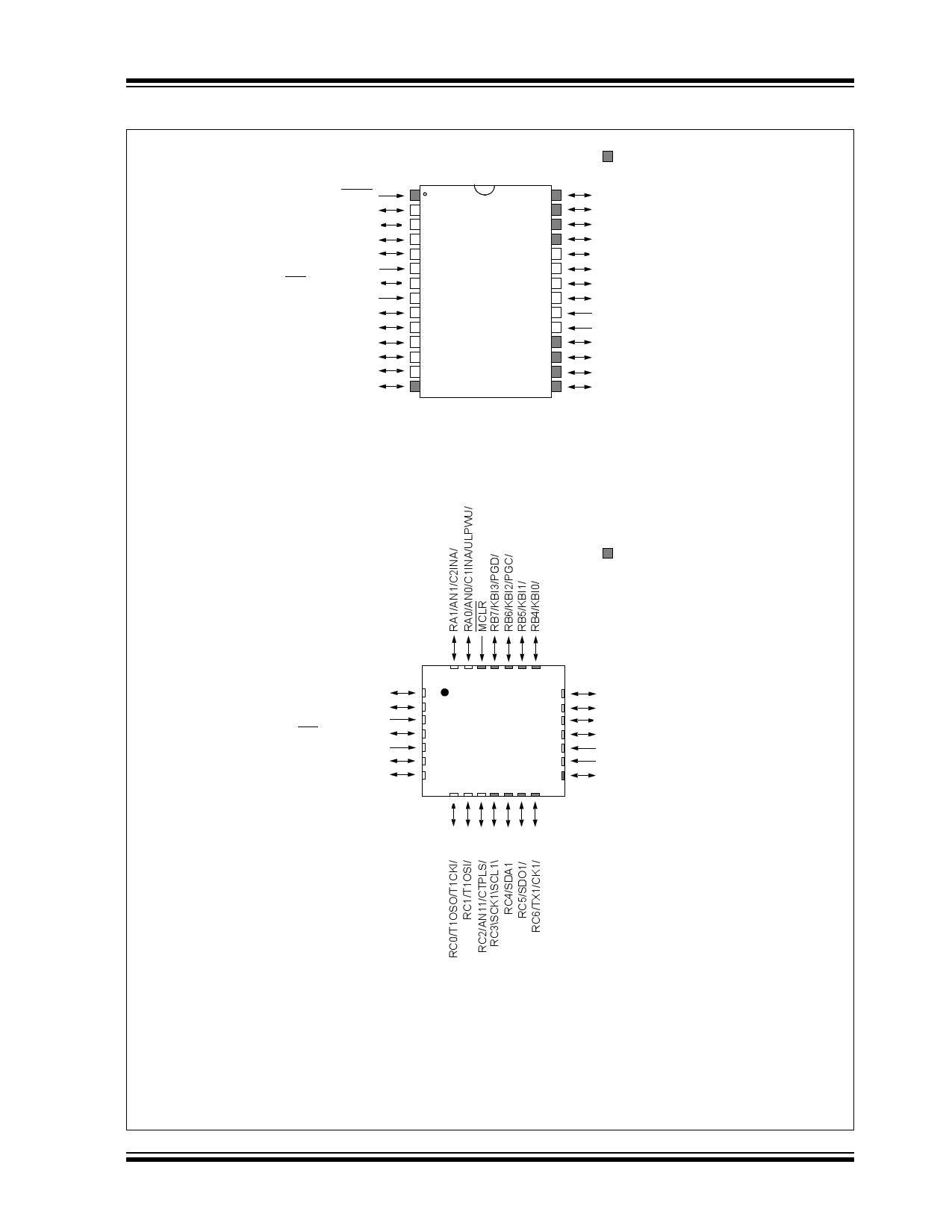
Pin Diagrams
28-Pin SPDIP/SOIC/SSOP(1)
MCLR
RA0/AN0/C1INA/ULPWU/RP0
RA1/AN1/C2INA/RP1
RA2/AN2/VREF-/CVREF/C2INB
RA3/AN3/VREF+/C1INB
VDDCORE/VCAP(2)
RA5/AN4/SS1/HLVDIN/RP2
VSS
OSC1/CLKI/RA7
OSC2/CLKO/RA6
RC0/T1OSO/T1CKI/RP11
RC1/T1OSI/RP12
RC2/AN11/CTPLS/RP13
RC3/SCK1/SCL1/RP14
1
2
3
4
5
6
7
8
9
10
11
12
13
14
PIC18F46J11 FAMILY
= Pins are up to 5.5V tolerant
28 RB7/KBI3/PGD/RP10
27 RB6/KBI2/PGC/RP9
26 RB5/KBI1/RP8
25 RB4/KBI0/RP7
24 RB3/AN9/CTED2/RP6
23 RB2/AN8/CTED1/REFO/RP5
22 RB1/AN10/RTCC/RP4
21 RB0/AN12/INT0/RP3
20 VDD
19 VSS
18 RC7/RX1/DT1/RP18
17 RC6/TX1/CK1/RP17
16 RC5/SDO1/RP16
15 RC4/SDI1/SDA1/RP15
28-Pin QFN(1,3)
= Pins are up to 5.5V tolerant
RA2/AN2/VREF-/CVREF/C2INB
RA3/AN3/VREF+/C1INB
VDDCORE/VCAP(2)
RA5/AN4/SS1/HLVDIN/RP2
VSS
OSC1/CLKI/RA7
OSC2/CLKO/RA6
28 27 26 25 24 23 22
1 21
2 20
3 19
4 PIC18F2XJ11 18
5 17
6 16
7 15
8 9 1011 12 13 14
RB3/AN9/CTED2/RP6
RB2/AN8/CTED1/REFO/RP5
RB1/AN10/RTCC/RP4
RB0/AN12/INT0/RP3
VDD
VSS
RC7/RX1/DT1/RP18
Legend:
Note 1:
2:
3:
RPn represents remappable pins.
Some input and output functions are routed through the Peripheral Pin Select (PPS) module and can be
dynamically assigned to any of the RPn pins. For a list of the input and output functions, see Table 10-13
and Table 10-14, respectively. For details on configuring the PPS module, see Section 10.7 “Peripheral
Pin Select (PPS)”.
See Section 26.3 “On-Chip Voltage Regulator” for details on how to connect the VDDCORE/VCAP pin.
For the QFN package, it is recommended that the bottom pad be connected to VSS.
2011 Microchip Technology Inc.
DS39932D-page 5
5 Page 
PIC18F46J11 FAMILY
1.0 DEVICE OVERVIEW
This document contains device-specific information for
the following devices:
• PIC18F24J11
• PIC18F25J11
• PIC18F26J11
• PIC18F44J11
• PIC18F45J11
• PIC18F46J11
• PIC18LF24J11
• PIC18LF25J11
• PIC18LF26J11
• PIC18LF44J11
• PIC18LF45J11
• PIC18LF46J11
1.1 Core Features
1.1.1 nanoWatt TECHNOLOGY
All of the devices in the PIC18F46J11 family incorporate
a range of features that can significantly reduce power
consumption during operation. Key features are:
• Alternate Run Modes: By clocking the controller
from the Timer1 source or the internal RC
oscillator, power consumption during code
execution can be reduced by as much as 90%.
• Multiple Idle Modes: The controller can also run
with its CPU core disabled but the peripherals still
active. In these states, power consumption can be
reduced even further, to as little as 4% of normal
operational requirements.
• On-the-Fly Mode Switching: The
power-managed modes are invoked by user code
during operation, allowing the users to incorporate
power-saving ideas into their application’s
software design.
1.1.2
OSCILLATOR OPTIONS AND
FEATURES
All of the devices in the PIC18F46J11 family offer five
different oscillator options, allowing users a range of
choices in developing application hardware. These
include:
• Two Crystal modes using crystals or ceramic
resonators.
• Two External Clock modes offering the option of a
divide-by-4 clock output.
• An internal oscillator block, which provides an
8 MHz clock and an INTRC source (approxi-
mately 31 kHz, stable over temperature and VDD),
as well as a range of six user-selectable clock
frequencies, between 125 kHz to 4 MHz, for a
total of eight clock frequencies. This option frees
an oscillator pin for use as an additional general
purpose I/O.
• A Phase Lock Loop (PLL) frequency multiplier,
available to the high-speed crystal, and external
and internal oscillators, providing a clock speed
up to 48 MHz.
The internal oscillator block provides a stable reference
source that gives the PIC18F46J11 family additional
features for robust operation:
• Fail-Safe Clock Monitor: This option constantly
monitors the main clock source against a reference
signal provided by the internal oscillator. If a clock
failure occurs, the controller is switched to the
internal oscillator, allowing for continued low-speed
operation or a safe application shutdown.
• Two-Speed Start-up: This option allows the
internal oscillator to serve as the clock source
from Power-on Reset (POR), or wake-up from
Sleep mode, until the primary clock source is
available.
1.1.3 EXPANDED MEMORY
The PIC18F46J11 family provides ample room for
application code, from 16 Kbytes to 64 Kbytes of code
space. The Flash cells for program memory are rated
to last in excess of 10000 erase/write cycles. Data
retention without refresh is conservatively estimated to
be greater than 20 years.
The Flash program memory is readable and writable
during normal operation. The PIC18F46J11 family also
provides plenty of room for dynamic application data
with up to 3.8 Kbytes of data RAM.
2011 Microchip Technology Inc.
DS39932D-page 11
11 Page | ||
| Páginas | Total 30 Páginas | |
| PDF Descargar | [ Datasheet PIC18LF44J11.PDF ] | |
Hoja de datos destacado
| Número de pieza | Descripción | Fabricantes |
| PIC18LF44J10 | RISC Microcontrollers | Microchip Technology |
| PIC18LF44J11 | High-Performance Microcontrollers | Microchip Technology |
| Número de pieza | Descripción | Fabricantes |
| SLA6805M | High Voltage 3 phase Motor Driver IC. |
Sanken |
| SDC1742 | 12- and 14-Bit Hybrid Synchro / Resolver-to-Digital Converters. |
Analog Devices |
|
DataSheet.es es una pagina web que funciona como un repositorio de manuales o hoja de datos de muchos de los productos más populares, |
| DataSheet.es | 2020 | Privacy Policy | Contacto | Buscar |
