|
|
|
PDF UVIS25TR Data sheet ( Hoja de datos )
| Número de pieza | UVIS25TR | |
| Descripción | Digital UV Index sensor | |
| Fabricantes | STMicroelectronics | |
| Logotipo | ||
Hay una vista previa y un enlace de descarga de UVIS25TR (archivo pdf) en la parte inferior de esta página. Total 26 Páginas | ||
|
No Preview Available !
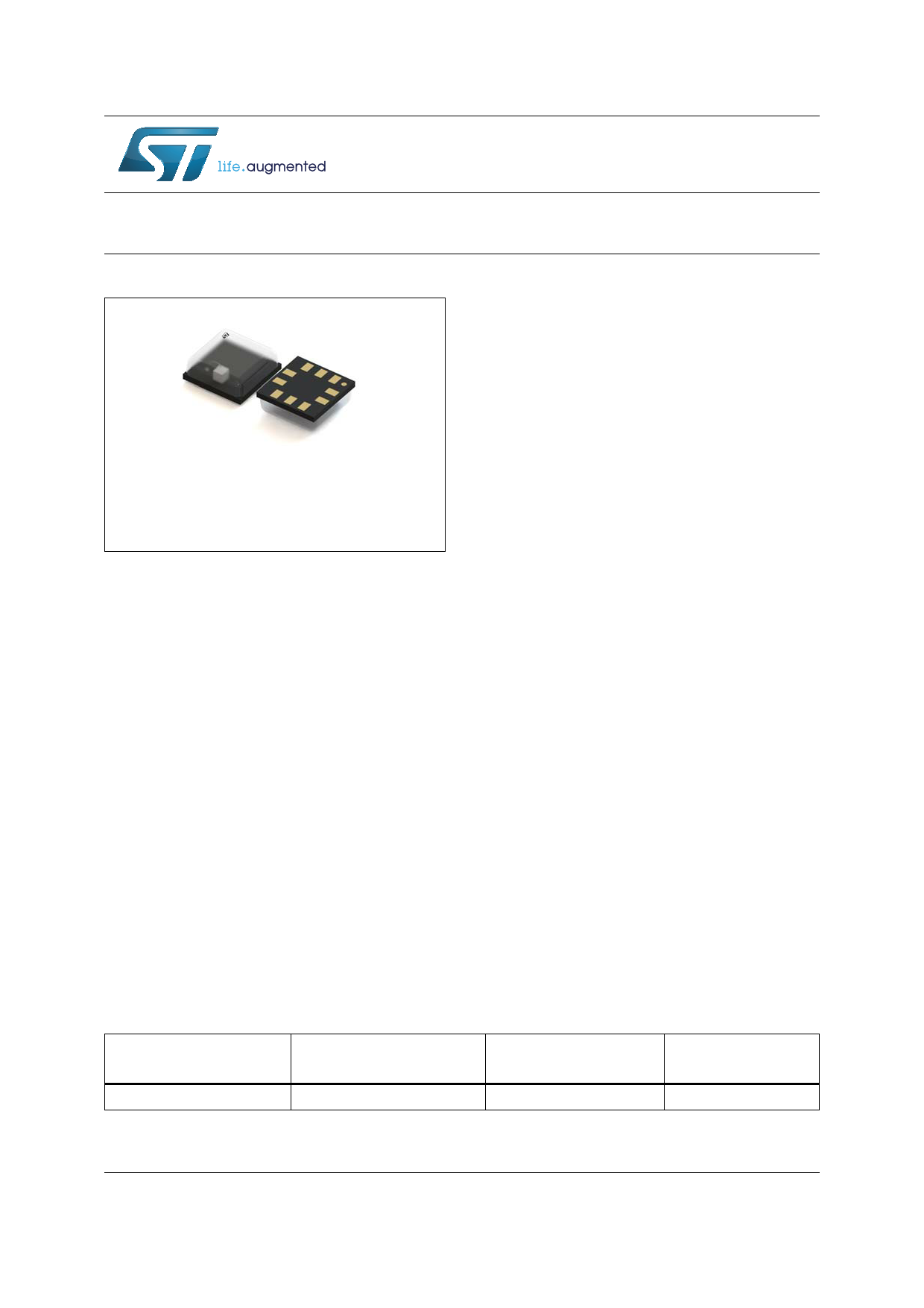
UVIS25
Digital UV Index sensor: 0 - 15 UV Index output range
Datasheet - preliminary data
LGA-10L
(2.5 x 2.5 x 0.76 mm)
Features
• 0 - 15 UV Index output range
• Resolution: UVI/16
• Active and power down modes
• Continuous reading at 1 Hz ODR / one shot
mode
• Interrupt functions: Data Ready and UVI
thresholds
• SPI and I²C interfaces
• Supply voltage: 1.7 to 3.6 V
• ECOPACK® lead-free compliant
Description
The UVIS25 is a digital UV Index sensor able to
provide an accurate measurement of the
Ultraviolet radiation index (UVI) from the sunlight.
It includes a sensing element and a mixed signal
ASIC to provide the UV Index data trough I2C and
SPI interfaces.
A dedicated technology has been developed to
achieve the best accuracy for UV Index
measurements.
The UVIS25 allows the measurement of the UV
Index, without the need of a dedicated algorithm
to calculate the UV Index and without specific
calibrations at customer manufacturing line.
The device can be configured to generate
interrupt events based on a threshold crossing or
when a new set of data is generated. The event is
available in a register as well as in a dedicated
pin.
The UVIS25 is available in a full-mold LGA
package (LGA). It is guaranteed to operate over a
temperature range extending from -20°C to
+85°C. The package is transparent to allow
external solar radiation to reach the sensing
element.
Applications
• UV Index measurements
• Wearable devices
• Smartphone and tablet
• Weather stations
Order code
UVIS25TR
Table 1. Device summary
Temperature range
[°C]
Package
-20 to +85
LGA-10L
Packing
Tape and reel
February 2015
DocID027323 Rev 1
This is preliminary information on a new product now in development or undergoing evaluation. Details are subject to
change without notice.
1/26
www.st.com
1 page 
UVIS25
Block diagram and pin description
Pin
number
1
2
3
4
5
6
7
8
9
10
Table 2. Pin description
Name
Function
VDD_IO Power supply for I/O pins
SCL
SPC
I²C serial clock (SCL)
SPI serial port clock (SPC)
Reserved Connect to GND
SDA
SDI
SDI/SDO
I²C serial data (SDA)
4-wire SPI serial data input (SDI)
3-wire serial data input /output (SDI/SDO)
SDO 4-wire SPI serial data output (SDO)
SPI enable
CS I²C/SPI mode selection
(1: SPI idle mode / I²C communication enabled; 0: SPI communication
mode / I²C disabled)
INT_DRDY Interrupt or Data Ready
GND 0 V supply
GND 0 V supply
VDD
Power supply
DocID027323 Rev 1
5/26
26
5 Page 
UVIS25
Digital interfaces
5.1.1
I²C operation
The transaction on the bus is started through a START (ST) signal. A start condition is
defined as a HIGH to LOW transition on the data line while the SCL line is held HIGH. After
this has been transmitted by the master, the bus is considered busy. The next data byte
transmitted after the start condition contains the address of the slave in the first 7 bits and
the eighth bit tells whether the master is receiving data from the slave or transmitting data to
the slave. When an address is sent, each device in the system compares the first seven bits
after a start condition with its address. If they match, the device considers itself addressed
by the master.
The slave address (SAD) associated to the UVIS25 is 1000111 (47h).
Data transfer with acknowledge is mandatory. The transmitter must release the SDA line
during the acknowledge pulse. The receiver must then pull the data line LOW so that it
remains stable low during the HIGH period of the acknowledge clock pulse. A receiver
which has been addressed is obliged to generate an acknowledge after each byte of data
received.
The I²C embedded in the UVIS25 behaves like a slave device and the following protocol
must be adhered to. After the start condition (ST) a slave address is sent, once a slave
acknowledge (SAK) has been returned, a 8-bit sub-address (SUB) will be transmitted: the 7
LSB represents the actual register address while the MSB enables address auto increment.
If the MSb of the SUB field is '1', the SUB (register address) will be automatically increased
to allow multiple data read/write.
The slave address is completed with a Read/Write bit: 1000111b If the bit "b" is set to'1'
(Read), a repeated START (SR) condition must be issued after the two sub-address bytes; if
the bit "b" is '0' (Write) the master will transmit to the slave with direction unchanged. Table 8
explains how the SAD+read/write bit pattern is composed, listing all the possible
configurations.
Command
Read
Write
Table 8. SAD+Read/Write patterns
SAD[7:1]
R/W
1000111
1000111
1
0
SAD+R/W
1000111 (8Fh)
1000111 (8Eh)
Master
Slave
Table 9. Transfer when master is writing one byte to slave
ST SAD + W
SUB
DATA
SAK
SAK
SAK
SP
Master
Slave
Table 10. Transfer when master is writing multiple bytes to slave
ST SAD + W
SUB
DATA
DATA
SAK
SAK
SAK
SAK
SP
Table 11. Transfer when master is receiving (reading) one byte of data from slave
Master ST SAD + W
SUB
SR SAD + R
NMAK
Slave
SAK
SAK
SAK DATA
SP
DocID027323 Rev 1
11/26
26
11 Page | ||
| Páginas | Total 26 Páginas | |
| PDF Descargar | [ Datasheet UVIS25TR.PDF ] | |
Hoja de datos destacado
| Número de pieza | Descripción | Fabricantes |
| UVIS25TR | Digital UV Index sensor | STMicroelectronics |
| Número de pieza | Descripción | Fabricantes |
| SLA6805M | High Voltage 3 phase Motor Driver IC. |
Sanken |
| SDC1742 | 12- and 14-Bit Hybrid Synchro / Resolver-to-Digital Converters. |
Analog Devices |
|
DataSheet.es es una pagina web que funciona como un repositorio de manuales o hoja de datos de muchos de los productos más populares, |
| DataSheet.es | 2020 | Privacy Policy | Contacto | Buscar |