|
|
|
PDF GL494 Data sheet ( Hoja de datos )
| Número de pieza | GL494 | |
| Descripción | PWM CONTROL CIRCUIT | |
| Fabricantes | Hynix Semiconductor | |
| Logotipo | ||
1. GL494 Hay una vista previa y un enlace de descarga de GL494 (archivo pdf) en la parte inferior de esta página. Total 7 Páginas | ||
|
No Preview Available !
GL494
GL494
PWM CONTROL CIRCUIT
Description
The GL494 incorporates on a single monolithic chip all the
functions required in the construction of a pulse-width-
modulation control circuit. Designed primarily for power
supply control, the GL494 contains an on-chip 5-volt
regulator, two error amplifiers, adjustable oscillator, dead-
time control comparator, pulse-steering flip-flop, and
output-control circuitry. The uncommitted output
transistors pro-vide either common-emitter or emitter-
follower output capability. Push-pull or single-ended
output operation may be selected through the output-
control function. The ar-chitecture of the GL494 prohibits
the possibility of either output being pulsed twice during
push-pull operation.
Features
— Complete PWM Power Control Circuitry
— Uncommitted Outputs for 200mA Sink or Source
— Output Control Selects Single-Ended or Push-Pull
Operation
— Internal Circuitry Prohibits Double Pulse at Either
Output
— Internal Regulator Provides a Stable 5V Reference
Supply
— Variable Dead-Time Provides Control Over Total
Range
Pin Configuration
NONINV INPUT
INV. INPUT
FEEDBACK
DEAD TIME CONTROL
Cr
Rr
GND
C1
1
2
3
4
5
6
7
8
16 NON INV INPUT
15 INV. INPUT
14 REF. OUT
13 OUTPUT CONTROL
12 Vcc
11 C2
10 E2
9 E1
Function Table
Output Control
Grounded
At Vref
Output Function
Single-ended or Parallel Output
Normal Push-Pull Operation
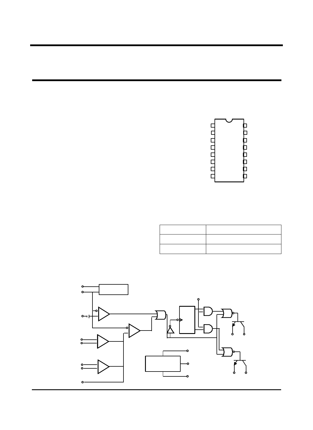
Block Diagram
RT
CT OSCILLATOR
DEAD 0.1V
TIME
CONTROL (4)
ERROR AMPLIFIERS
NONINVERTING(1)
INPUT
+
INVERTING (2)
−
INPUT
ERROR AMP1
NONINVERTING(16)
INPUT
INVERTING (15)
INPUT
(3)
FEEDBACK
+
−
ERROR AMP2
OUTPUT
CONTROL
(See Function Table)
PULSE STEERING
(13)
FLIP FLOP
Q
T
PWM
COMPARATOR
Q
REFERENCE
REGULATOR
VCC
(12)
REF OUT
(14)
GND
(7)
E1(9) C1(8)
E1(10) C2(11)
1
1 page 
GL494
Parameter Measurement Information
1.Dead time and Feedback Control
Vcc=15V
TEST
DEAD TIME (4)
(8) C1
INPUTS
12kΩ FEEDBACK (3)
Re (6)
(9) E1
Cr (5)
(11) C2
0.01µF (+) (16) ERROR (12) E2
(-) (15) AMP
(+) (1) ERROR
50kΩ
(-) (2) AMP
OUTPUT
(14) REF
CONTROL GND (7) OUT
(13)
TEST CIRCUIT
150Ω
2W
150Ω
2W
OUTPUT 1
VOLTAGE
AT C1
VOLTAGE
AT C2
OUTPUT 2
VOLTAGE
AT CT
THRESHOLD VOLTAGE
DEAD-TIME
CONTROL
INTPUT
0V
THRESHOLD VOLTAGE
Vcc
0
Vcc
0
FEEDBACK 0.7V
DUTY
CYCLE
MAX
0%
VOLTAGE
MAX
WAVEFORMS
0%
2. Error Amplifier Characteristics
V1
VREF
ERROR AMPLIFIER
+ UNDER TEST
FEEDBACK
TERMINAL
–
+
– OTHER
ERROR
AMPLIFIER
3. Common-Emitter Configuration
(EACH OUTPUT
CIRCUIT)
15V
68Ω
2W
OUTPUT
90%
90%
CL=15pF
(INCLUDES PROBE AND
JIG CAPACITANCE)
10%
tr
10%
tf
TEST CIRCUIT
OUTPUT VOLTAGE WAVEFORM
5
5 Page | ||
| Páginas | Total 7 Páginas | |
| PDF Descargar | [ Datasheet GL494.PDF ] | |
Hoja de datos destacado
| Número de pieza | Descripción | Fabricantes |
| GL4910 | Side View Type Infrared Emitting Diode for Camera AF (Automatic Focusing) | Sharp Electrionic Components |
| GL494 | PWM CONTROL CIRCUIT | Hynix Semiconductor |
| GL496 | High Speed Infrared Emitting Diode | Sharp Electrionic Components |
| Número de pieza | Descripción | Fabricantes |
| SLA6805M | High Voltage 3 phase Motor Driver IC. |
Sanken |
| SDC1742 | 12- and 14-Bit Hybrid Synchro / Resolver-to-Digital Converters. |
Analog Devices |
|
DataSheet.es es una pagina web que funciona como un repositorio de manuales o hoja de datos de muchos de los productos más populares, |
| DataSheet.es | 2020 | Privacy Policy | Contacto | Buscar |