|
|
|
PDF MMSZ5242BT1G Data sheet ( Hoja de datos )
| Número de pieza | MMSZ5242BT1G | |
| Descripción | Zener Voltage Regulators | |
| Fabricantes | ON Semiconductor | |
| Logotipo | ||
Hay una vista previa y un enlace de descarga de MMSZ5242BT1G (archivo pdf) en la parte inferior de esta página. Total 7 Páginas | ||
|
No Preview Available !
MMSZ52xxxT1G Series,
SZMMSZ52xxxT1G Series
Zener Voltage Regulators
500 mW SOD−123 Surface Mount
Three complete series of Zener diodes are offered in the convenient,
surface mount plastic SOD−123 package. These devices provide a
convenient alternative to the leadless 34−package style.
Features
• 500 mW Rating on FR−4 or FR−5 Board
• Wide Zener Reverse Voltage Range − 2.4 V to 110 V
• Package Designed for Optimal Automated Board Assembly
• Small Package Size for High Density Applications
• General Purpose, Medium Current
• ESD Rating of Class 3 (> 16 kV) per Human Body Model
• SZ Prefix for Automotive and Other Applications Requiring Unique
Site and Control Change Requirements; AEC−Q101 Qualified and
PPAP Capable
• These are Pb−Free Devices*
Mechanical Characteristics:
CASE: Void-free, transfer-molded, thermosetting plastic case
FINISH: Corrosion resistant finish, easily solderable
MAXIMUM CASE TEMPERATURE FOR SOLDERING PURPOSES:
260°C for 10 Seconds
POLARITY: Cathode indicated by polarity band
FLAMMABILITY RATING: UL 94 V−0
MAXIMUM RATINGS
Rating
Symbol
Max
Units
Total Power Dissipation on FR−5 Board,
(Note 1) @ TL = 75°C
Derated above 75°C
PD
500 mW
6.7 mW/°C
Thermal Resistance, Junction−to−Ambient
(Note 2)
RqJA
340 °C/W
Thermal Resistance, Junction−to−Lead
(Note 2)
RqJL
150 °C/W
Junction and Storage Temperature Range TJ, Tstg −55 to +150 °C
Stresses exceeding Maximum Ratings may damage the device. Maximum
Ratings are stress ratings only. Functional operation above the Recommended
Operating Conditions is not implied. Extended exposure to stresses above the
Recommended Operating Conditions may affect device reliability.
1. FR−5 = 3.5 X 1.5 inches, using the minimum recommended footprint.
2. Thermal Resistance measurement obtained via infrared Scan Method.
*For additional information on our Pb−Free strategy and soldering details, please
download the ON Semiconductor Soldering and Mounting Techniques
Reference Manual, SOLDERRM/D.
© Semiconductor Components Industries, LLC, 2012
October, 2012 − Rev. 12
1
http://onsemi.com
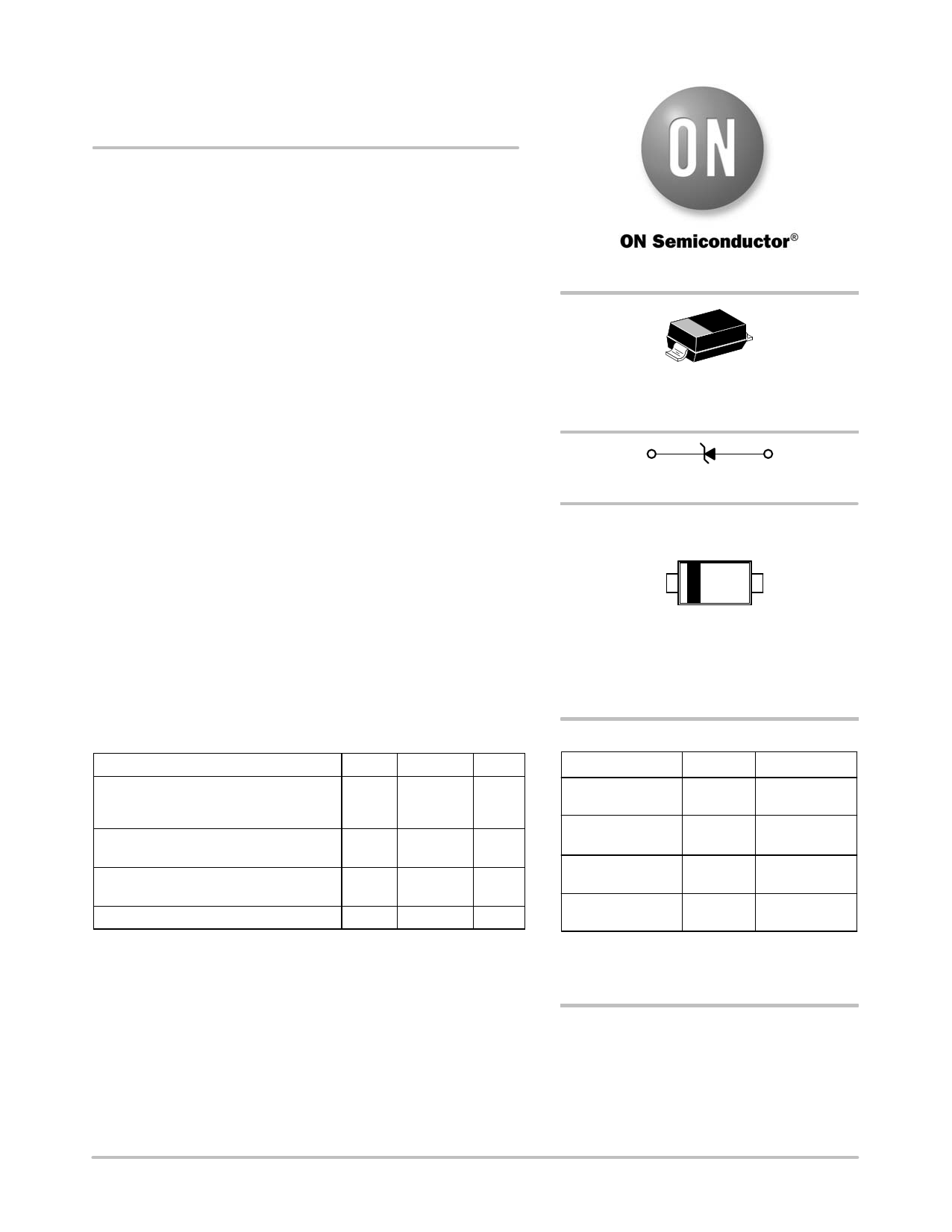
SOD−123
CASE 425
STYLE 1
1
Cathode
2
Anode
MARKING DIAGRAM
1
xx MG
G
xx = Device Code (Refer to page 3)
M = Date Code
G = Pb−Free Package
(Note: Microdot may be in either location)
ORDERING INFORMATION
Device
Package
Shipping†
MMSZ52xxBT1G, SOD−123
SZMMSZ52xxBT1G (Pb−Free)
3,000 /
Tape & Reel
MMSZ52xxCT1G, SOD−123
SZMMSZ52xxCT1G (Pb−Free)
3,000 /
Tape & Reel
MMSZ52xxBT3G, SOD−123
SZMMSZ52xxBT3G (Pb−Free)
10,000 /
Tape & Reel
MMSZ52xxCT3G, SOD−123
SZMMSZ52xxCT3G (Pb−Free)
10,000 /
Tape & Reel
†For information on tape and reel specifications,
including part orientation and tape sizes, please
refer to our Tape and Reel Packaging Specifications
Brochure, BRD8011/D.
DEVICE MARKING INFORMATION
See specific marking information in the device marking
column of the Electrical Characteristics table on page 3 of
this data sheet.
Publication Order Number:
MMSZ5221BT1/D
1 page 
MMSZ52xxxT1G Series, SZMMSZ52xxxT1G Series
TYPICAL CHARACTERISTICS
8
7 TYPICAL TC VALUES
6 FOR MMSZ52xxBT1G SERIES,
5 SZMMSZ52xxBT1G SERIES
4
3
2
1
0
VZ @ IZT
1000
100
TYPICAL TC VALUES
FOR MMSZ52xxBT1G SERIES,
SZMMSZ52xxBT1G SERIES
VZ @ IZT
10
−1
−2
−3 2
3
4 5 6 7 8 9 10
VZ, NOMINAL ZENER VOLTAGE (V)
11 12
110
100
VZ, NOMINAL ZENER VOLTAGE (V)
200
Figure 1. Temperature Coefficients
(Temperature Range − 55°C to +150°C)
Figure 2. Temperature Coefficients
(Temperature Range − 55°C to +150°C)
1.2
1.0
0.8 PD versus TL
0.6 PD versus TA
0.4
0.2
00
25 50 75 100 125
T, TEMPERATURE (°C)
Figure 3. Steady State Power Derating
1000
100
RECTANGULAR
WAVEFORM, TA = 25°C
10
150 1 0.1
1 10 100
PW, PULSE WIDTH (ms)
1000
Figure 4. Maximum Nonrepetitive Surge Power
1000
IZ = 1 mA
100
5 mA
20 mA
10
TJ = 25°C
IZ(AC) = 0.1 IZ(DC)
f = 1 kHz
1000
100
75 V (MMSZ5267BT1G)
91 V (MMSZ5270BT1G)
10
150°C 75°C 25°C 0°C
11
1
10 100 0.4 0.5 0.6 0.7 0.8 0.9 1.0 1.1 1.2
VZ, NOMINAL ZENER VOLTAGE
VF, FORWARD VOLTAGE (V)
Figure 5. Effect of Zener Voltage on
Zener Impedance
Figure 6. Typical Forward Voltage
http://onsemi.com
5
5 Page | ||
| Páginas | Total 7 Páginas | |
| PDF Descargar | [ Datasheet MMSZ5242BT1G.PDF ] | |
Hoja de datos destacado
| Número de pieza | Descripción | Fabricantes |
| MMSZ5242BT1 | Zener Voltage Regulators | ON |
| MMSZ5242BT1G | Zener Voltage Regulators | ON Semiconductor |
| Número de pieza | Descripción | Fabricantes |
| SLA6805M | High Voltage 3 phase Motor Driver IC. |
Sanken |
| SDC1742 | 12- and 14-Bit Hybrid Synchro / Resolver-to-Digital Converters. |
Analog Devices |
|
DataSheet.es es una pagina web que funciona como un repositorio de manuales o hoja de datos de muchos de los productos más populares, |
| DataSheet.es | 2020 | Privacy Policy | Contacto | Buscar |