|
|
|
PDF XC6227 Data sheet ( Hoja de datos )
| Número de pieza | XC6227 | |
| Descripción | 700mA High Speed LDO Regulator | |
| Fabricantes | Torex Semiconductor | |
| Logotipo | ||
1. XC6227 Hay una vista previa y un enlace de descarga de XC6227 (archivo pdf) en la parte inferior de esta página. Total 25 Páginas | ||
|
No Preview Available !
XC6227 Series
700mA High Speed LDO Regulator with Reverse Current Protection
ETR0354-004
■GENERAL DESCRIPTION
The XC6227 series is a highly accurate, low noise, high ripple rejection, low dropout, and low power consumption high speed
voltage regulator.
The series consists of a voltage reference, an error amplifier, a driver transistor, a current limiter, a thermal protection circuit, a
reverse current protection circuit and a phase compensation circuit.
The CE function enables the entire circuit to be placed in a stand-by state by inputting a low level signal to the CE pin.
Over-current protection and thermal protection circuits are integrated. The protection circuit starts to operate when either output
current reaches the current limit level or junction temperature reaches the temperature limit. With the reverse current protection
function of a driver transistor, the reverse current flow is prohibited when VOUT voltage is higher than VIN voltage. For an example,
when a battery is connected to the VOUT pin, battery current will not flow back to the XC6227.
■APPLICATIONS
● USB products and HDMI equipments
● E-book Readers / Electronic dictionaries
● Smart Phones / Mobile phones
● Portable game consoles
● Modules (Wireless, Camera, etc.)
■FEATURES
Maximum Output Current
Dropout Voltage
Operating Voltage Range
Output Voltages
Accuracy
Low Power Consumption
Chip Enable(CE)
: 700mA
: 120mV @IOUT=300mA(VOUT=3.0V)
: 1.7V ~ 6.0V
: 0.8V~5.0V (0.05V increments)
: +1% (VOUT>2.0V)
+0.02V (VOUT≦2.0V)
: 100μA
: Active High
Standby Current below 0.1μA
High Ripple Rejection
: 65dB @ 1kHz
Operating Ambient Temperature : -40℃~+85℃
Low ESR Capacitor
: Ceramic capacitor
Packages
: USP-6C, SOT-25, SOT-89-5
Environmentally Friendly : EU RoHS Compliant, Pb Free
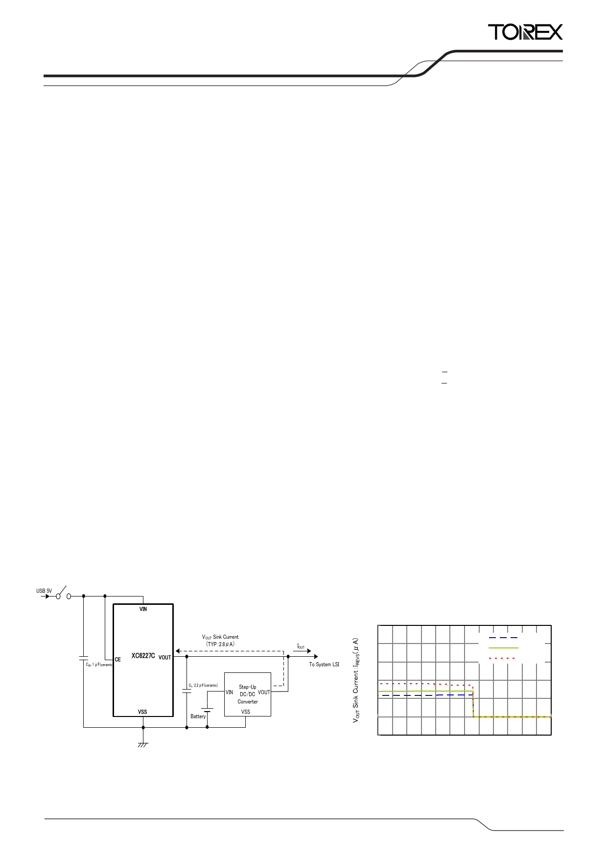
■TYPICAL APPLICATION CIRCUIT ■ TYPICAL PERFORMANCE
CHARACTERISTICS
●●逆V流OU時T SViOnUkT端Cu子rrシenンt VクS電. I流np-u入t V力o電lta圧ge特性例
XC6227C331
VOUT=3.3V
IOUT=0mA
10
-40℃
8 25℃
6 85℃
4
2
0
-2
0 0.5 1 1.5 2 2.5 3 3.5 4 4.5 5 5.5 6
Input Voltage:VIN(V)
1/25
1 page 
XC6227
Series
■OUTPUT VOLTAGE CHART
●Voltage Chart 1
NOMINAL
OUTPUT
VOLTAGE
(V)
VOUT(T)
0.80
0.85
0.90
0.95
1.00
1.05
1.10
1.15
1.20
1.25
1.30
1.35
1.40
1.45
1.50
1.55
1.60
1.65
1.70
1.75
1.80
1.85
1.90
1.95
2.00
2.05
2.10
2.15
2.20
2.25
2.30
2.35
2.40
2.45
2.50
2.55
2.60
2.65
2.70
2.75
2.80
2.85
2.90
2.95
3.00
OUTPUT VOLTAGE
(V)
VOUT(E)
MIN.
MAX.
0.7800
0.8300
0.8800
0.9300
0.9800
1.0300
1.0800
1.1300
1.1800
1.2300
1.2800
1.3300
1.3800
1.4300
1.4800
1.5300
1.5800
1.6300
1.6800
1.7300
1.7800
1.8300
1.8800
1.9300
1.9800
2.0295
2.0790
2.1285
2.1780
2.2275
2.2770
2.3265
2.3760
2.4255
2.4750
2.5245
2.5740
2.6235
2.6730
2.7225
2.7720
2.8215
2.8710
2.9205
2.9700
0.8200
0.8700
0.9200
0.9700
1.0200
1.0700
1.1200
1.1700
1.2200
1.2700
1.3200
1.3700
1.4200
1.4700
1.5200
1.5700
1.6200
1.6700
1.7200
1.7700
1.8200
1.8700
1.9200
1.9700
2.0200
2.0705
2.1210
2.1715
2.2220
2.2725
2.3230
2.3735
2.4240
2.4745
2.5250
2.5755
2.6260
2.6765
2.7270
2.7775
2.8280
2.8785
2.9290
2.9795
3.0300
LOAD REGULATION
E-1 (mV)
∆VOUT
TYP.
MAX.
25 50
25 50
25 50
25 50
25 50
30 60
30 60
30 60
30 60
30 60
30 60
30 60
30 60
30 60
30 60
30 60
30 60
30 60
30 60
30 60
30 60
30 60
30 60
30 60
30 60
35 70
35 70
35 70
35 70
35 70
35 70
35 70
35 70
35 70
35 70
35 70
35 70
35 70
35 70
35 70
35 70
35 70
35 70
35 70
43 85
DROPOUT VOLTAGE 1 DROPOUT VOLTAGE 2
E-2 (mV)
Vdif
MAX.
TYP.
720 880
720 880
720 880
720 880
570 740
570 740
570 740
570 740
420 570
420 570
420 570
420 570
320 470
320 470
280 410
280 410
280 410
280 410
280 410
280 410
220 350
220 350
220 350
220 350
200 320
200 320
200 320
200 320
200 320
200 320
200 320
200 320
200 320
200 320
160 260
160 260
160 260
160 260
160 260
160 260
160 260
160 260
160 260
160 260
120 200
E-3 (mV)
Vdif2
MAX.
TYP.
230 510
230 510
230 510
230 510
75 260
75 260
75 260
75 260
50 135
40 80
40 80
40 80
40 80
40 80
40 80
40 80
40 80
40 80
40 80
40 80
40 80
40 80
40 80
40 80
40 80
40 80
40 80
40 80
40 80
40 80
40 80
40 80
40 80
40 80
40 80
40 80
40 80
40 80
40 80
40 80
40 80
40 80
40 80
40 80
40 80
5/25
5 Page 
■■特T性YP例ICAL PERFORMANCE CHARACTERISTICS (Continued)
((11)) O出u力tpu電t V圧olt-ag出e 力vs.電Ou流tp特ut 性Cu例rrent (Continued)
XC6227
Series
6.0
5.0
4.0
3.0
2.0
1.0
0.0
0
XC6227x501
VIN = 6.0V
CIN = 1.0μF (ceramic),CL=2.2μF(ceramic)
-40℃
25℃
85℃
200 400 600 800 1000 1200
Output Current: IOUT [mA]
6.0
5.0
4.0
3.0
2.0
1.0
0.0
0
XC6227x501
Ta = 25℃
CIN = 1.0μF (ceramic),CL=2.2μF(ceramic)
VIN=5.1V
VIN=5.3V
VIN=5.5V
VIN=6.0V
200 400 600 800 1000 1200
Output Current: IOUT [mA]
((22)) O出u力tpu電t V圧olt-ag入e 力vs.電In圧put特Vo性lta例ge
XC6227x081
Ta = 25℃
1.0 CIN = 1.0μF (ceramic),CL=6.8μF(ceramic)
0.8
0.6
0.4
0.2
0.0
0.0
IOUT=0.1mA
IOUT=10mA
IOUT=30mA
IOUT=100mA
1.0 2.0 3.0 4.0 5.0
Input Voltage: VIN [V]
6.0
XC6227x151
Ta = 25℃
2.0 CIN = 1.0μF (ceramic),CL=6.8μF(ceramic)
1.5
1.0
0.5
0.0
0.0
IOUT=0.1mA
IOUT=10mA
IOUT=30mA
IOUT=100mA
1.0 2.0 3.0 4.0 5.0
Input Voltage: VIN [V]
6.0
0.90
0.85
0.80
0.75
0.70
0.65
2.0
XC6227x081
Ta = 25℃
CIN = 1.0μF (ceramic),CL=6.8μF(ceramic)
IOUT=0.1mA
IOUT=10mA
IOUT=30mA
IOUT=100mA
3.0 4.0 5.0
Input Voltage: VIN [V]
6.0
1.60
1.55
1.50
1.45
1.40
1.35
2.0
XC6227x151
Ta = 25℃
CIN = 1.0μF (ceramic),CL=6.8μF(ceramic)
IOUT=0.1mA
IOUT=10mA
IOUT=30mA
IOUT=100mA
3.0 4.0 5.0
Input Voltage: VIN [V]
6.0
11/25
11 Page | ||
| Páginas | Total 25 Páginas | |
| PDF Descargar | [ Datasheet XC6227.PDF ] | |
Hoja de datos destacado
| Número de pieza | Descripción | Fabricantes |
| XC6220 | 1A LDO Voltage Regulator | Torex Semiconductor |
| XC6221 | Low ESR Caps Compatible High Speed LDO Voltage Regulators | Torex Semiconductor |
| XC6222 | 700mA High Speed LDO Regulator | Torex Semiconductor |
| XC6223 | 300mA High Speed LDO Voltage Regulator | Torex Semiconductor |
| Número de pieza | Descripción | Fabricantes |
| SLA6805M | High Voltage 3 phase Motor Driver IC. |
Sanken |
| SDC1742 | 12- and 14-Bit Hybrid Synchro / Resolver-to-Digital Converters. |
Analog Devices |
|
DataSheet.es es una pagina web que funciona como un repositorio de manuales o hoja de datos de muchos de los productos más populares, |
| DataSheet.es | 2020 | Privacy Policy | Contacto | Buscar |