|
|
|
PDF CY7C038-20AC Data sheet ( Hoja de datos )
| Número de pieza | CY7C038-20AC | |
| Descripción | Dual-Port Static RAM | |
| Fabricantes | Cypress Semiconductor | |
| Logotipo | ||
Hay una vista previa y un enlace de descarga de CY7C038-20AC (archivo pdf) en la parte inferior de esta página. Total 19 Páginas | ||
|
No Preview Available !
25/0251
CY7C027/028
CY7C037/038
Features
• True Dual-Ported memory cells which allow simulta-
neous access of the same memory location
• 32K x 16 organization (CY7C027)
• 64K x 16 organization (CY7C028)
• 32K x 18 organization (CY7C037)
• 64K x 18 organization (CY7C038)
• 0.35-micron CMOS for optimum speed/power
• High-speed access: 12[1]/15/20 ns
• Low operating power
— Active: ICC = 180 mA (typical)
— Standby: ISB3 = 0.05 mA (typical)
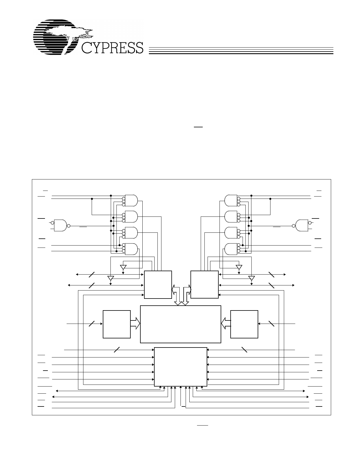
Logic Block Diagram
R/WL
UBL
32K/64K x 16/18
Dual-Port Static RAM
• Fully asynchronous operation
• Automatic power-down
• Expandable data bus to 32/36 bits or more using Mas-
ter/Slave chip select when using more than one device
• On-chip arbitration logic
• Semaphores included to permit software handshaking
between ports
• INT flags for port-to-port communication
• Separate upper-byte and lower-byte control
• Dual Chip Enables
• Pin select for Master or Slave
• Commercial and industrial temperature ranges
• Available in 100-pin TQFP
• Pin-compatible and functionally equivalent to IDT7027
R/WR
UBR
CE0L
CE1L
LBL
OEL
CEL
[2]
I/O8/9L–I/O15/17L
[3]
I/O0L–I/O7/8L
8/9
8/9
I/O
Control
I/O
Control
CER
CE0R
CE1R
LBR
OER
8/9 [2]
I/O8/9L–I/O15/17R
8/9 [3]
I/O0L–I/O7/8R
[4]
A0L–A14/15L
15/16
Address
Decode
True Dual-Ported
RAM Array
Address
Decode
15/16
[4]
A0R–A14/15R
[4]
A0L–A14/15L
15/16
15/16
[4]
A0R–A14/15R
CEL Interrupt CER
OEL Semaphore
OER
R/WL
SEML
BUSYL[5]
INTL
UBL
LBL
Arbitration
M/S
R/WR
SEMR
[5]
BUSYR
INTR
UBR
LBR
Notes:
1. See page 6 for Load Conditions.
2. I/O8–I/O15 for x16 devices; I/O9–I/O17 for x18 devices.
3. I/O0–I/O7 for x16 devices; I/O0–I/O8 for x18 devices.
4. A0–A14 for 32K; A0–A15 for 64K devices.
5. BUSY is an output in master mode and an input in slave mode.
For the most recent information, visit the Cypress web site at www.cypress.com
Cypress Semiconductor Corporation • 3901 North First Street • San Jose • CA 95134 • 408-943-2600
Document #: 38-06042 Rev. *A
Revised December 27, 2002
1 page 
CY7C027/028
CY7C037/038
Electrical Characteristics Over the Operating Range
Symbol
VOH
VOL
VIH
VIL
IOZ
ICC
ISB1
ISB2
ISB3
ISB4
Parameter
Output HIGH Voltage (VCC=Min.,
IOH= –4.0 mA)
Output LOW Voltage (VCC=Min.,
IOH= +4.0 mA)
Input HIGH Voltage
Input LOW Voltage
Output Leakage Current
Operating Current
(VCC=Max, IOUT=0 mA)
Outputs Disabled
Com’l.
Ind.[10]
Standby Current (Both
Ports TTL Level) CEL & CER
≥ VIH, f=fMAX
Standby Current (One Port
TTL Level) CEL | CER ≥ VIH,
f=fMAX
Standby Current (Both
Ports CMOS Level) CEL &
CER ≥ VCC – 0.2V, f=0
Standby Current (One Port
CMOS Level)
VIH, f=fMAX[11]
CEL
|
CER
≥
Com’l.
Ind.[10]
Com’l.
Ind.[10]
Com’l.
Ind.[10]
Com’l.
Ind.[10]
Min.
2.4
2.2
–10
-12[1]
Typ.
195
55
125
0.05
115
Max.
0.4
0.8
10
325
75
205
0.5
185
CY7C027/028
CY7C037/038
-15
Min. Typ. Max.
2.4
0.4
2.2
0.8
–10 10
190 280
50 70
120 180
0.05 0.5
110 160
Min.
2.4
2.2
–10
-20
Typ.
180
305
45
60
110
125
0.05
0.05
100
115
Max.
0.4
0.8
10
265
290
65
80
160
175
0.5
0.5
140
155
Unit
V
V
V
V
µA
mA
mA
mA
mA
mA
mA
mA
mA
mA
mA
Note:
11. fMAX = 1/tRC = All inputs cycling at f = 1/tRC (except output enable). f = 0 means no address or control lines change. This applies only to inputs at CMOS level standby ISB3.
Document #: 38-06042 Rev. *A
Page 5 of 19
5 Page 
CY7C027/028
CY7C037/038
Switching Waveforms (continued)
Semaphore Read After Write Timing, Either Side[37]
A0–A 2
SEM
VALID ADRESS
tAW
tSCE
tHA
tSAA
VALID ADRESS
tSOP
tACE
tOHA
I/O0
R/W
OE
tSD
DATAIN VALID
tSA
tPWE
tHD
DATAOUT VALID
WRITE CYCLE
tSWRD
tSOP
tDOE
READ CYCLE
Timing Diagram of Semaphore Contention[38, 39, 40]
A0L –A2L
MATCH
R/WL
SEM L
A 0R–A2R
R/WR
SEM R
tSPS
MATCH
Notes:
37. CE = HIGH for the duration of the above timing (both write and read cycle).
38. I/O0R = I/O0L = LOW (request semaphore); CER = CEL = HIGH.
39. Semaphores are reset (available to both ports) at cycle start.
40. If tSPS is violated, the semaphore will definitely be obtained by one side or the other, but which side will get the semaphore is unpredictable.
Document #: 38-06042 Rev. *A
Page 11 of 19
11 Page | ||
| Páginas | Total 19 Páginas | |
| PDF Descargar | [ Datasheet CY7C038-20AC.PDF ] | |
Hoja de datos destacado
| Número de pieza | Descripción | Fabricantes |
| CY7C038-20AC | Dual-Port Static RAM | Cypress Semiconductor |
| CY7C038-20AI | Dual-Port Static RAM | Cypress Semiconductor |
| Número de pieza | Descripción | Fabricantes |
| SLA6805M | High Voltage 3 phase Motor Driver IC. |
Sanken |
| SDC1742 | 12- and 14-Bit Hybrid Synchro / Resolver-to-Digital Converters. |
Analog Devices |
|
DataSheet.es es una pagina web que funciona como un repositorio de manuales o hoja de datos de muchos de los productos más populares, |
| DataSheet.es | 2020 | Privacy Policy | Contacto | Buscar |