|
|
|
PDF CY7C027-20AXIT Data sheet ( Hoja de datos )
| Número de pieza | CY7C027-20AXIT | |
| Descripción | 32K / 64K x 16 Dual-Port Static RAM | |
| Fabricantes | Cypress Semiconductor | |
| Logotipo | ||
Hay una vista previa y un enlace de descarga de CY7C027-20AXIT (archivo pdf) en la parte inferior de esta página. Total 23 Páginas | ||
|
No Preview Available !
CY7C02732 K / 64 K × 16 Dual-Port Static RAM
CY7C027
CY7C028
32 K / 64 K × 16 Dual-Port Static RAM
32 K / 64 K × 16 Dual-Port Static RAM
Features
■ True dual-ported memory cells which allow simultaneous
access of the same memory location
■ 32 K × 16 organization (CY7C027)
■ 64 K × 16 organization (CY7C028)
■ 0.35 micron CMOS for optimum speed and power
■ High speed access: 15 and 20 ns
■ Low operating power
■ Active: ICC = 180 mA (typical)
■ Standby: ISB3 = 0.05 mA (typical)
■ Fully asynchronous operation
■ Automatic power down
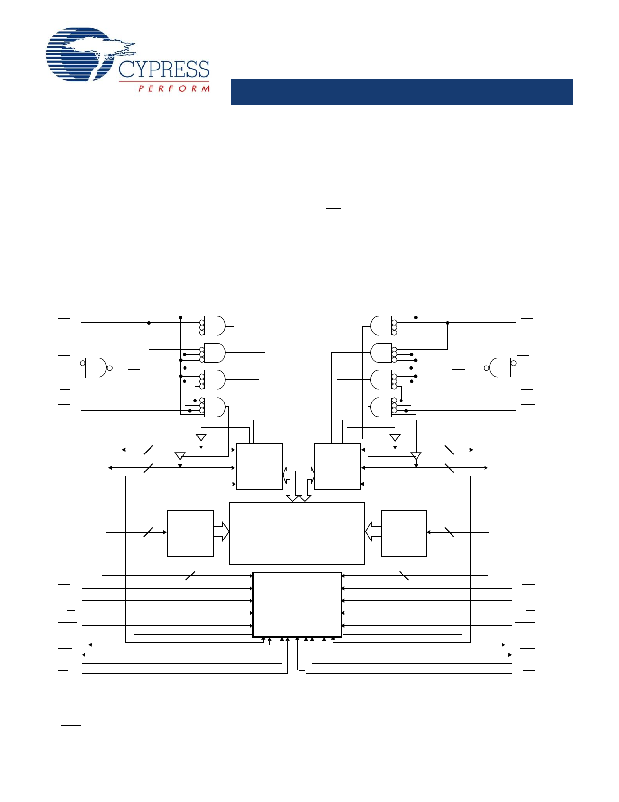
Logic Block Diagram
R/WL
UBL
■ Expandable data bus to 32 bits or more using Master/Slave
chip select when using more than one device
■ On-chip arbitration logic
■ Semaphores included to permit software handshaking
between ports
■ INT flags for port-to-port communication
■ Separate upper-byte and lower-byte control
■ Dual chip enables
■ Pin select for Master or Slave
■ Commercial and industrial temperature ranges
■ Available in 100-pin TQFP
■ Pb-free packages available
R/WR
UBR
CE0L
CE1L
LBL
OEL
CEL
I/O8L–I/O15[1L]
I/O0L–I/O[72L]
8
8
I/O
Control
I/O
Control
CER
CE0R
CE1R
LBR
OER
8 I/O8L–I/[O1]15R
8 I/O0L–I/O[2]7R
A0L–A[134]/15L
15/16
Address
Decode
True Dual-Ported
RAM Array
Address
Decode
15/16
A0R–A[134] /15R
A0L–A[134]/15L
CEL
OEL
R/WL
SEML
BUSYL[4]
INTL
UBL
LBL
15/16
Notes
1. I/O8–I/O15 for × 16 devices
2. I/O0–I/O7 for × 16 devices
3. A0–A14 for 32K; A0–A15 for 64K devices.
4. BUSY is an output in master mode and an input in slave mode.
Interrupt
Semaphore
Arbitration
M/S
15/16
A0R–A[134] /15R
CER
OER
R/WR
SEMR
[4] BUSYR
INTR
UBR
LBR
Cypress Semiconductor Corporation • 198 Champion Court
Document Number: 38-06042 Rev. *J
• San Jose, CA 95134-1709 • 408-943-2600
Revised August 28, 2013
1 page 
CY7C027
CY7C028
Selection Guide
Parameter
Maximum Access Time
Typical Operating Current
Typical Standby Current for ISB1 (Both ports TTL level)
Typical Standby Current for ISB3 (Both ports CMOS level)
CY7C027/CY7C028
-15
15
190
50
0.05
CY7C027/CY7C028
-20
20
180
45
0.05
Unit
ns
mA
mA
mA
Pin Definitions
Left Port
CE0L, CE1L
R/WL
OEL
A0L–A15L
I/O0L–I/O15L
SEML
UBL
LBL
INTL
BUSYL
M/S
VCC
GND
NC
Right Port
CE0R, CE1R
R/WR
OER
A0R–A15R
I/O0R–I/O15R
SEMR
UBR
LBR
INTR
BUSYR
Description
Chip Enable (CE is LOW when CE0 VIL and CE1 VIH)
Read/Write Enable
Output Enable
Address (A0–A14 for 32K; A0–A15 for 64K devices)
Data Bus Input/Output (I/O0–I/O15 for × 16 devices)
Semaphore Enable
Upper Byte Select (I/O8–I/O15 for × 16 devices)
Lower Byte Select (I/O0–I/O7 for × 16 devices)
Interrupt Flag
Busy Flag
Master or Slave Select
Power
Ground
No Connect
Document Number: 38-06042 Rev. *J
Page 5 of 23
5 Page 
CY7C027
CY7C028
Switching Waveforms (continued)
Figure 7. Write Cycle No. 1 (R/W Controlled Timing) [25, 26, 27, 28]
ADDRESS
tWC
OE
CE [29, 30]
R/W
DATA OUT
DATA IN
tAW
tSA tPWE[28]
NOTE 32
tHZWE[31]
tSD
tHA
tLZWE
tHD
tHZOE[31]
NOTE 32
ADDRESS
CE [29, 30]
R/W
Figure 8. Write Cycle No. 2 (CE Controlled Timing) [25, 26, 27, 32, 33]
tWC
tAW
tSA
tSCE
tHA
DATA IN
tSD tHD
Notes
25. R/W must be HIGH during all address transitions.
26. A write occurs during the overlap (tSCE or tPWE) of a LOW CE or SEM and a LOW UB or LB.
27. tHA is measured from the earlier of CE or R/W or (SEM or R/W) going HIGH at the end of write cycle.
28.
If OE
to be
short
is LOW during a R/W controlled write cycle,
placed on the bus for the
as the specified tPWE.
required
tSD.
If
OE
the write pulse
is HIGH during
width must be the
an R/W controlled
lwarrgiteercoyfctleP,WtEhiosrre(tqHuZiWreEm+entStDd)oteosanllootwatphpelyI/aOnddrtihveerws rtiotetuprunlsoeffcaanndbdeaatas
29. To access RAM, CE = VIL, SEM = VIH.
30.
To
To
access
access
upper
lower
byte,
byte,
CE
CE
=
=
VVIILL,,
LUBB==VVILIL,,SSEEMM==VVIHIH..
31. Transition is measured 500 mV from steady state with a 5 pF load (including scope and jig). This parameter is sampled and not 100% tested.
32. During this period, the I/O pins are in the output state, and input signals must not be applied.
33. If the CE or SEM LOW transition occurs simultaneously with or after the R/W LOW transition, the outputs remain in the high impedance state.
Document Number: 38-06042 Rev. *J
Page 11 of 23
11 Page | ||
| Páginas | Total 23 Páginas | |
| PDF Descargar | [ Datasheet CY7C027-20AXIT.PDF ] | |
Hoja de datos destacado
| Número de pieza | Descripción | Fabricantes |
| CY7C027-20AXI | 32K / 64K x 16 Dual-Port Static RAM | Cypress Semiconductor |
| CY7C027-20AXIT | 32K / 64K x 16 Dual-Port Static RAM | Cypress Semiconductor |
| Número de pieza | Descripción | Fabricantes |
| SLA6805M | High Voltage 3 phase Motor Driver IC. |
Sanken |
| SDC1742 | 12- and 14-Bit Hybrid Synchro / Resolver-to-Digital Converters. |
Analog Devices |
|
DataSheet.es es una pagina web que funciona como un repositorio de manuales o hoja de datos de muchos de los productos más populares, |
| DataSheet.es | 2020 | Privacy Policy | Contacto | Buscar |