No Preview Available !

18W Hi-Fi AMPLIFIER AND
35W DRIVER
DESCRIPTION
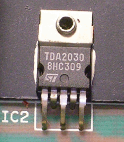
The TDA2030 is a monolithic IC in Pentawatt package
intended for use as low frequency class AB amplifier.
With Vsmax=44V it is particularly suited for more reliable
applications withou regulated supply and for 35W driver
circuits using lowcost complementary pairs.
The TDA2030 provides high output current and has very
low harmonic and cross-over distortion.
Further the device incorporates a short circuit protection
system somprising an arrangement for automatically limiting
the dissipated power to as to keep the working point of the
output transistors within their safe operating area. A
conventional thermal system is also included.
ABSOLUTE MAXIMUM RATINGS(Ta=25°C)
CHARACTERISTICS
SYMBOL
Supply Voltage
Vs
Input Voltage
Vi
Differential input voltage
Vdi
Peak output current(internally limited)
Io
Total power dissipation at Tcase=90°�
Ptot
Storage temperature
Tstg
junction temperature
Tj
VALUE
±22
Vs
±15
3.5
20
-40~+150
-40~+150
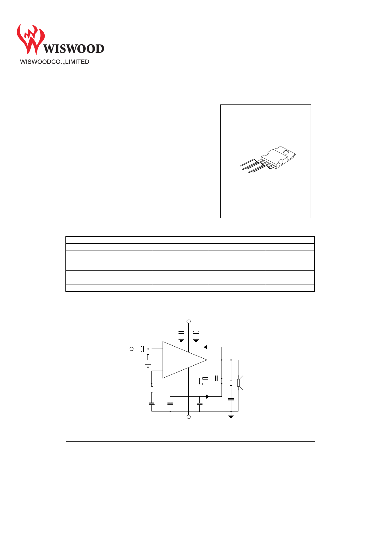
TYPICAL APPLICATION
+Vs
C5
C1 100nF
Vi 1µF
1
5
R3
22kΩ TDA2030
C3
100µF
D1
1N4001
4
2
3
R5
C8 R4
1Ω
R3
680Ω
R1 D1
22kΩ 1N4001
C2
22µF
C6
100µF
C4 C7
100nF 220nF
-Vs
RL
TO-220
UNITS
V
V
V
A
W
°C
°C
1

TDA2030
Gv 140
(dB)
100
60
20
Fig.2 Open loop frequency
response
Phase
Gain
180
90
0
Po 24
(W)
20
16
12
Fig.3 Output power vs. Supply
voltage
Gv=26dB
d=0.5%
f=40 to 15kHz
RL=4Ω
RL=8Ω
-20
-60
1
10
2
10
34
10 10
5 67
10 10 10
Frequency (Hz)
d 102
(%)
Fig.4 Total harmonic distortion
vs. output power
101 Gv=26dB
100
10-1
-2
10
10-2
30
Vo
(Vp-p)
25
Vs=38V
RL=8Ω
f=15kHz
f=1kHz
Vs=32V
RL=4Ω
10-1 100
101 102
Po (W)
Fig.6 Large signal frequency
response
Vs=±15V
RL=8Ω
Vs=±15V
20 RL=4Ω
15
10
5
101
102 103 104
Frequency (kHz)
8
4
24
d 102
(%)
101
28 32 36 40 44
Vs (V)
Fig.5 Two tone CCIF
intermodulation distortion
Po (W)
Vs=32V
100
Po=4W
RL=4Ω
Gv=26dB
10-1 Order (2f1-f2)
Order (2f2-f1)
10-2
101
30
Ptot
(W)
25
102 103
104 105
Frequency (Hz)
Fig.7 Maximum allowable power
dissipation vs. ambient
temperture
20
15 hRetaht=si8hRnekktah/h=tWsa4inkvki/nWhgaving
10
5
-50
0
50 100
150 200
Tamb (k)
5

TDA2030
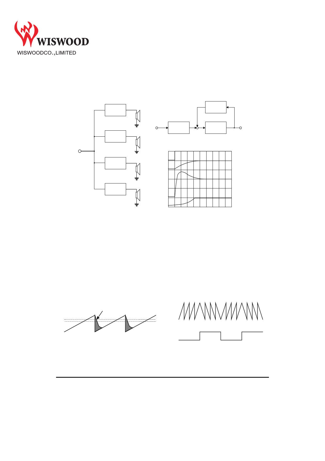
Fig.21 High power active box for musical
instrument
20 to 40W
Amplifier
20 to 40W
Amplifier
Fig.22 Overshoot phenomenon in
feedback amplifiers
FEEDBACK
PATH
βV4
INPUT
PRE
V1 AMPLIFIER V2
POWER
OUTPUT
V3 AMPLIFIER V4
20 to 40W
Amplifier
V1
V2
20 to 40W
Amplifier
V3
V4
method for the measurement of TIM consicts of feeding sine waves superimposed onto square wavers,into the
amplifier under test.The output spectrum is then examined using a spectrum analyser and compared to the
input.This method suffers from serious disadvantages:the accuracy is limited, the measurement is a tather delicate
operation and an expensive spectrum analyser is essential.A new approach (see Technical Note 143(Applied by
SGS to monolithic amplifiers measurement is fast cheap,it requires nothing more sophisticated than an
oscilloscope-and sensitive-and it can be used down to the values as low as 0.002% in high power amplifiers.
The "inverting-sawtooth" method of measurement is based on the response of an amplifier to a 20KHz sawtooth
waveform.The amplifier has no difficulty following the slow ramp but it cannot follow the fast edge.The output will
follow the upper line in Fig.23 cutting of the shade area and thus increasing the mean level.If this output signal is
filtered to remove the sawtooth,direct voltage remains which indicates the amount of tIM distortion, although it is
difficult to measure because it is indistingishable from the DC offset of the amplifier.This problem os neatly avoided
in the IS-TIM method by periodically inverting the sawtooth waveform at a low audio frequency as shown in
Fig.24.Inthe case of the sawtooth in Fig. 25 the means level was increased by the TIM distortion, for a sawtooth in
the other direction the opposite is ture.
SR(V/µs)
m2
m1
Fig.23 20kHz sawtooth waveform
Input
Signal
Filtered
Output
Siganal
Fig.24 Inverting sawtooth waveform
11


