|
|
|
PDF 8N4QV01 Data sheet ( Hoja de datos )
| Número de pieza | 8N4QV01 | |
| Descripción | IDT8N4QV01 | |
| Fabricantes | Integrated Device Technology | |
| Logotipo | ||
Hay una vista previa y un enlace de descarga de 8N4QV01 (archivo pdf) en la parte inferior de esta página. Total 20 Páginas | ||
|
No Preview Available !
Quad-Frequency Programmable
VCXO
IDT8N4QV01 REV G
DATA SHEET
General Description
The IDT8N4QV01 is a Quad-Frequency Programmable VCXO with
very flexible frequency and pull-range programming capabilities.
The device uses IDT’s fourth generation FemtoClock® NG
technology for an optimum of high clock frequency and low phase
noise performance. The device accepts 2.5V or 3.3V supply and is
packaged in a small, lead-free (RoHS 6) 10-lead ceramic 5mm x
7mm x 1.55mm package.
Besides the 4 default power-up frequencies set by the FSEL0 and
FSEL1 pins, the IDT8N4QV01 can be programmed via the I2C
interface to any output clock frequency between 15.476MHz to
866.67MHz and from 975MHz to 1,300MHz to a very high degree of
precision with a frequency step size of 435.9Hz ÷N (N is the PLL
output divider). Since the FSEL0 and FSEL1 pins are mapped to 4
independent PLL, P, M and N divider registers (P, MINT, MFRAC
and N), reprogramming those registers to other frequencies under
control of FSEL0 and FSEL1 is supported. The extended
temperature range supports wireless infrastructure, tele-
communication and networking end equipment requirements.
Features
• Fourth generation FemtoClock® NG technology
• Programmable clock output frequency from 15.476MHz to
866.67MHz and from 975MHz to 1,300MHz
• Four power-up default frequencies (see part number order
codes), re-programmable by I2C
• I2C programming interface for the output clock frequency, APR
and internal PLL control registers
• Frequency programming resolution is 435.9Hz ÷N
• Absolute pull-range (APR) programmable from ±4.5ppm to
±754.5ppm
• One 2.5V or 3.3V LVDS differential clock output
• Two control inputs for the power-up default frequency
• LVCMOS/LVTTL compatible control inputs
• RMS phase jitter @ 156.25MHz (12kHz - 20MHz): 0.494ps
(typical)
• RMS phase jitter @ 156.25MHz (1kHz - 40MHz): 0.594ps
(typical)
• 2.5V or 3.3V supply voltage modes
• -40°C to 85°C ambient operating temperature
• Available in Lead-free (RoHS 6) package
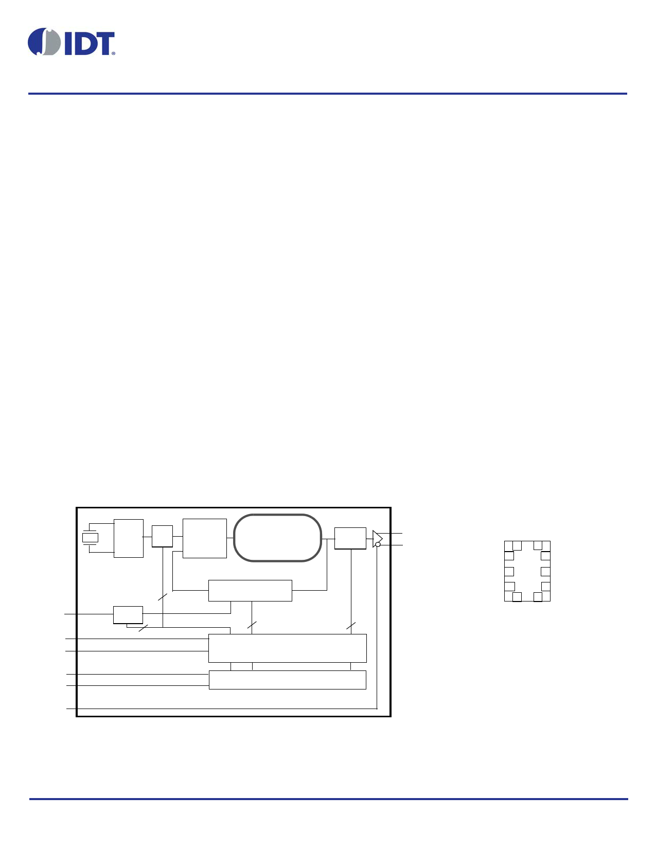
Block Diagram
OSC ÷P
114.285 MHz
VC
FSEL1
FSEL0
SCLK
SDATA
OE
Pulldown
Pulldown
A/D
2
7
Pullup
Pullup
Pullup
PFD FemtoClock® NG
&
VCO
÷N
LPF 1950-2600MHz
÷MINT, MFRAC
25
Configuration Register (ROM)
(Frequency, APR, Polarity)
7
I2C Control
Pin Assignment
Q
nQ
VC 1
8 VDD
OE 2
7 nQ
GND 3
6Q
IDT8N4QV01 REV G DATA SHEET
10-lead ceramic 5mm x 7mm x 1.55mm
package body
CD Package
Top View
IDT8N4QV01GCD MARCH 6, 2012 1 ©2012 Integrated Device Technology, Inc.
1 page 
IDT8N4QV01 REV G DATA SHEET
QUAD-FREQUENCY PROGRAMMABLE-VCXO
Principles of Operation
The block diagram consists of the internal 3rd overtone crystal and
oscillator which provide the reference clock fXTAL of either
114.285MHz or 100MHz. The PLL includes the FemtoClock NG VCO
along with the Pre-divider (P), the feedback divider (M) and the post
divider (N). The P, M, and N dividers determine the output frequency
based on the fXTAL reference and must be configured correctly for
proper operation. The feedback divider is fractional supporting a
huge number of output frequencies. The configuration of the
feedback divider to integer-only values results in an improved output
phase noise characteristics at the expense of the range of output
frequencies. In addition, internal registers are used to hold up to four
different factory pre-set P, M, and N configuration settings. These
default pre-sets are stored in the I2C registers at power-up. Each
configuration is selected via the the FSEL[1:0] pins and can be read
back using the SCLK and SDATA pins.
The user may choose to operate the device at an output frequency
different than that set by the factory. After power-up, the user may
write new P, N and M settings into one or more of the four
configuration registers and then use the FSEL[1:0] pins to select the
newly programmed configuration. Note that the I2C registers are
volatile and a power supply cycle will reload the pre-set factory
default conditions.
If the user does choose to write a different P, M, and N configuration,
it is recommended to write to a configuration which is not currently
selected by FSEL[1:0] and then change to that configuration after the
I2C transaction has completed. Changing the FSEL[1:0] controls
results in an immediate change of the output frequency to the
selected register values. The P, M, and N frequency configurations
support an output frequency range 15.476MHz to 866.67MHz and
975MHz to 1,300MHz.
The devices use the fractional feedback divider with a delta-sigma
modulator for noise shaping and robust frequency synthesis
capability. The relatively high reference frequency minimizes phase
noise generated by frequency multiplication and allows more efficient
shaping of noise by the delta-sigma modulator.
The output frequency is determined by the 2-bit pre-divider (P), the
feedback divider (M) and the 7-bit post divider (N). The feedback
divider (M) consists of both a 7-bit integer portion (MINT) and an
18-bit fractional portion (MFRAC) and provides the means for
high-resolution frequency generation. The output frequency fOUT is
calculated by:
As identified previously, the configurations of P, M (MINT & MFRAC)
and N divider settings are stored the I2C register, and the
configuration loaded at power-up is determined by the FSEL[1:0]
pins.
Table 4 Frequency Selection
Input
FSEL1 FSEL0
Selects
0 (def.) 0 (def.) Frequency 0
0 1 Frequency 1
1 0 Frequency 2
1 1 Frequency 3
Register
P0, MINT0, MFRAC0, N0
P1, MINT1, MFRAC1, N1
P2, MINT2, MFRAC2, N2
P3, MINT3, MFRAC3, N3
Frequency Configuration
An order code is assigned to each frequency configuration
programmed by the factory (default frequencies). For more
information on the available default frequencies and order codes,
please see the Ordering Information Section in this document. For
available order codes, see the FemtoClock NG Ceramic-Package
XO and VCXO Ordering Product Information document.
For more information and guidelines on programming of the device
for custom frequency configurations, the register description, the
pull-range programming and the serial interface description, see the
FemtoClock NG Ceramic 5x7 Module Programming Guide.
fOUT = fXTAL P-----1----N--
MINT + M------F----R----A----C-----+-----0---.--5-
218
(1)
The four configuration registers for the P, M (MINT & MFRAC) and N
dividers which are named Pn, MINTn, MFRACn and Nn with n = 0 to
3. “n” denominates one of the four possible configurations.
IDT8N4QV01GCD MARCH 6, 2012 5 ©2012 Integrated Device Technology, Inc.
5 Page 
IDT8N4QV01 REV G DATA SHEET
Parameter Measurement Information
QUAD-FREQUENCY PROGRAMMABLE-VCXO
3.3V±5%
POWER SUPPLY
+ Float GND –
VDD
SCOPE
Q
nQ
2.5V±5%
POWER SUPPLY
+ Float GND –
VDD
SCOPE
Q
nQ
3.3V LVDS Output Load AC Test Circuit
2.5V LVDS Output Load AC Test Circuit
Phase Noise Plot
f1 Offset Frequency f2
RMS Jitter = Area Under Curve Defined by the Offset Frequency Markers
RMS Phase Jitter
VOH
VREF
1σ contains 68.26% of all measurements
2σ contains 95.4% of all measurements
3σ contains 99.73% of all measurements
4σ contains 99.99366% of all measurements
6σ contains (100-1.973x10⁻⁷)% of all measurements
Reference Point
(Trigger Edge)
Histogram
Mean Period
(First edge after trigger)
VOL
Period Jitter
nQ
Q
t PW
t
PERIOD
odc = t PW x 100%
t PERIOD
Output Duty Cycle/Pulse Width/Period
nQ
Q
tcycle n
➤
tcycle n+1
| |tjit(cc) = tcycle n – tcycle n+1
1000 Cycles
➤
Cycle-to-Cycle Jitter
IDT8N4QV01GCD MARCH 6, 2012 11 ©2012 Integrated Device Technology, Inc.
11 Page | ||
| Páginas | Total 20 Páginas | |
| PDF Descargar | [ Datasheet 8N4QV01.PDF ] | |
Hoja de datos destacado
| Número de pieza | Descripción | Fabricantes |
| 8N4QV01 | IDT8N4QV01 | Integrated Device Technology |
| Número de pieza | Descripción | Fabricantes |
| SLA6805M | High Voltage 3 phase Motor Driver IC. |
Sanken |
| SDC1742 | 12- and 14-Bit Hybrid Synchro / Resolver-to-Digital Converters. |
Analog Devices |
|
DataSheet.es es una pagina web que funciona como un repositorio de manuales o hoja de datos de muchos de los productos más populares, |
| DataSheet.es | 2020 | Privacy Policy | Contacto | Buscar |