|
|
|
PDF AT25128 Data sheet ( Hoja de datos )
| Número de pieza | AT25128 | |
| Descripción | SPI Serial EEPROMs | |
| Fabricantes | ATMEL Corporation | |
| Logotipo | ||
Hay una vista previa y un enlace de descarga de AT25128 (archivo pdf) en la parte inferior de esta página. Total 22 Páginas | ||
|
No Preview Available !
Features
• Serial Peripheral Interface (SPI) Compatible
• Supports SPI Modes 0 (0,0) and 3 (1,1)
• Low-voltage and Standard-voltage Operation
– 2.7 (VCC = 2.7V to 5.5V)
– 1.8 (VCC = 1.8V to 5.5V)
• 3 MHz Clock Rate
• 64-byte Page Mode and Byte Write Operation
• Block Write Protection
– Protect 1/4, 1/2, or Entire Array
• Write Protect (WP) Pin and Write Disable Instructions for
Both Hardware and Software Data Protection
• Self-timed Write Cycle (5 ms Typical)
• High-reliability
– Endurance: 100,000 Write Cycles
– Data Retention: >200 Years
• Automotive Grade, Extended Temperature and Lead-Free Devices Available
• 8-lead PDIP, 8-lead EIAJ SOIC, 8-lead and 16-lead JEDEC SOIC, 14-lead and 20-lead
TSSOP, and 8-lead Leadless Array Packages
Description
The AT25128/256 provides 131,072/262,144 bits of serial electrically-erasable pro-
grammable read only memory (EEPROM) organized as 16,384/32,768 words of 8 bits
each. The device is optimized for use in many industrial and commercial applications
where low-power and low-voltage operation are essential. The devices are available in
space saving 8-lead PDIP (AT25128/256), 8-lead EIAJ SOIC (AT25128/256), 8-lead
and 16-lead JEDEC SOIC (AT25128), 14-lead TSSOP (AT25128), 20-lead TSSOP
(AT25128/256), and 8-lead Leadless Array (AT25256) packages. In addition, the entire
family is available in 2.7V (2.7V to 5.5V) and 1.8V (1.8V to 5.5V) versions.
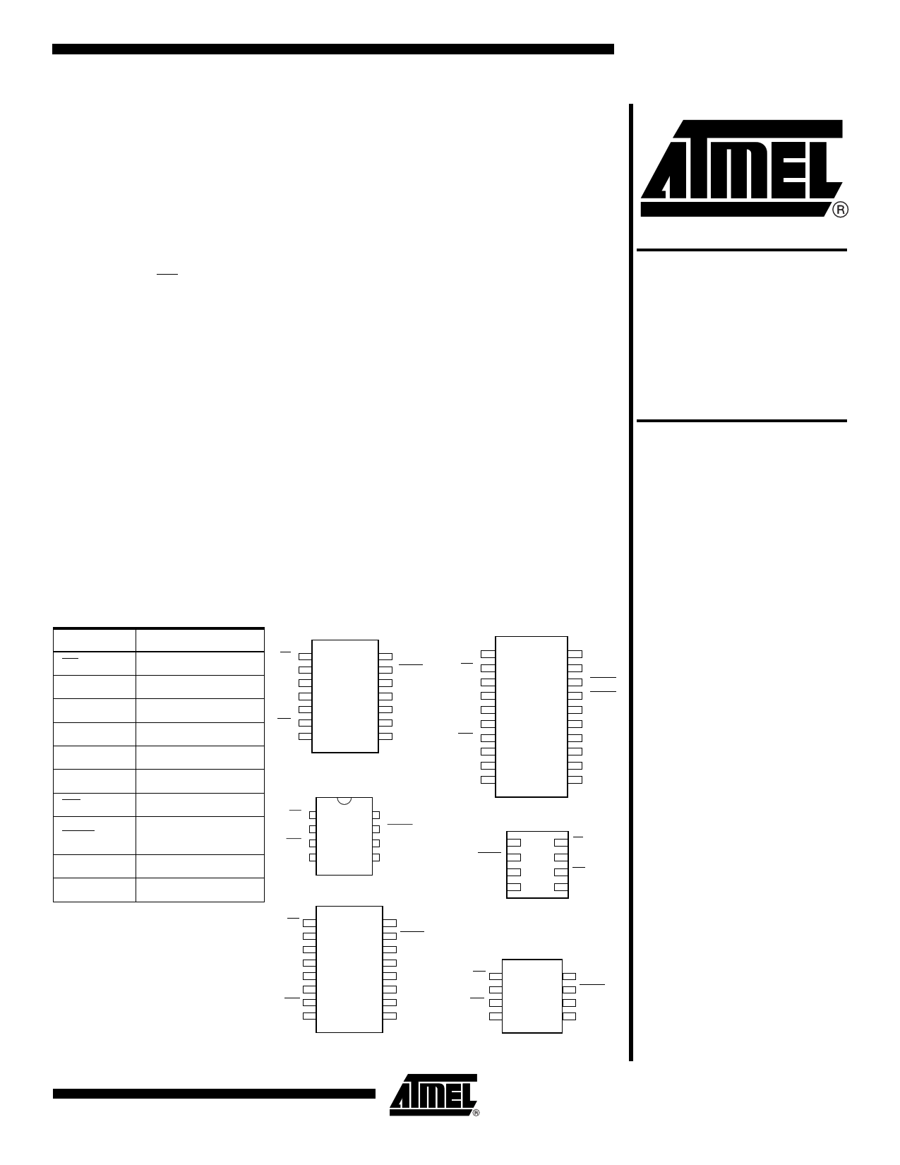
Table 1. Pin Configuration
Pin Name Function
CS Chip Select
SCK
Serial Data Clock
SI Serial Data Input
SO Serial Data Output
GND
Ground
VCC
Power Supply
14-lead TSSOP
CS
SO
NC
NC
NC
WP
GND
1
2
3
4
5
6
7
14 VCC
13 HOLD
12 NC
11 NC
10 NC
9 SCK
8 SI
8-lead PDIP
20-lead TSSOP*
NC
CS
SO
SO
NC
NC
WP
GND
DC
NC
1
2
3
4
5
6
7
8
9
10
20 NC
19 VCC
18 HOLD
17 HOLD
16 NC
15 NC
14 SCK
13 SI
12 DC
11 NC
WP
HOLD
NC
DC
Write Protect
Suspends Serial
Input
No Connect
Don't Connect
CS
SO
WP
GND
1
2
3
4
8 VCC
7 HOLD
6 SCK
5 SI
16-lead SOIC
CS
SO
NC
NC
NC
NC
WP
GND
1
2
3
4
5
6
7
8
16 VCC
15 HOLD
14 NC
13 NC
12 NC
11 NC
10 SCK
9 SI
8-lead Leadless Array
VCC 8
HOLD 7
SCK 6
SI 5
1 CS
2 SO
3 WP
4 GND
Bottom View
8-lead SOIC
CS
SO
WP
GND
1
2
3
4
8 VCC
7 HOLD
6 SCK
5 SI
*Note: Pins 3, 4 and 17, 18 are internally connected for 14-lead TSSOP socket compatibility.
SPI Serial
EEPROMs
128K (16,384 x 8)
256K (32,768 x 8)
AT25128(1)
AT25256(2)
Notes:
1. This device is not rec-
ommended for new
designs. Please refer
to AT25128A.
2. This device is not rec-
ommended for new
designs. Please refer
to AT25256A.
Rev. 0872O–SEEPR–03/05
1
Free Datasheet http://www.Datasheet4U.com
1 page 
AT25128/256
Table 4. AC Characteristics (Continued)
Applicable over recommended operating range from TAI = –40°C to + 85°C, TAE = –40°C to +125°C, VCC = As Specified,
CL = 1 TTL Gate and 100 pF (unless otherwise noted)
Symbol
Parameter
Voltage
Min Max Units
tHZ Hold to Output High Z
4.5 – 5.5
2.7 – 5.5
1.8 – 5.5
100
200 ns
300
tDIS Output Disable Time
4.5 – 5.5
2.7 – 5.5
1.8 – 5.5
200
250
1000
ns
tWC Write Cycle Time
4.5 – 5.5
2.7 – 5.5
1.8 – 5.5
5
10
10
Endurance(1) 5.0V, 25°C, Page Mode
100K
Note: 1. This parameter is characterized and is not 100% tested. Contact Atmel for further information.
ms
Write Cycles
Serial Interface
Description
MASTER: The device that generates the serial clock.
SLAVE: Because the serial clock pin (SCK) is always an input, the AT25128/256
always operates as a slave.
TRANSMITTER/RECEIVER: The AT25128/256 has separate pins designated for data
transmission (SO) and reception (SI).
MSB: The Most Significant Bit (MSB) is the first bit transmitted and received.
SERIAL OP-CODE: After the device is selected with CS going low, the first byte will
be received. This byte contains the op-code that defines the operations to be performed.
INVALID OP-CODE: If an invalid op-code is received, no data will be shifted into the
AT25128/256, and the serial output pin (SO) will remain in a high impedance state until
the falling edge of CS is detected again. This will reinitialize the serial communication.
CHIP SELECT: The AT25128/256 is selected when the CS pin is low. When the device
is not selected, data will not be accepted via the SI pin, and the serial output pin (SO)
will remain in a high impedance state.
HOLD: The HOLD pin is used in conjunction with the CS pin to select the AT25128/256.
When the device is selected and a serial sequence is underway, HOLD can be used to
pause the serial communication with the master device without resetting the serial
sequence. To pause, the HOLD pin must be brought low while the SCK pin is low. To
resume serial communication, the HOLD pin is brought high while the SCK pin is low
(SCK may still toggle during HOLD). Inputs to the SI pin will be ignored while the SO pin
is in the high impedance state.
WRITE PROTECT: The write protect pin (WP) will allow normal read/write operations
when held high. When the WP pin is brought low and WPEN bit is “1”, all write opera-
tions to the status register are inhibited. WP going low while CS is still low will interrupt a
write to the status register. If the internal write cycle has already been initiated, WP
going low will have no effect on any write operation to the status register. The WP pin
function is blocked when the WPEN bit in the status register is “0”. This will allow the
user to install the AT25128/256 in a system with the WP pin tied to ground and still be
able to write to the status register. All WP pin functions are enabled when the WPEN bit
is set to “1”.
0872O–SEEPR–03/05
5
Free Datasheet http://www.Datasheet4U.com
5 Page 
Figure 7. WRSR Timing
Figure 8. READ Timing
Figure 9. WRITE Timing
0872O–SEEPR–03/05
AT25128/256
11
Free Datasheet http://www.Datasheet4U.com
11 Page | ||
| Páginas | Total 22 Páginas | |
| PDF Descargar | [ Datasheet AT25128.PDF ] | |
Hoja de datos destacado
| Número de pieza | Descripción | Fabricantes |
| AT25128 | SPI Serial EEPROMs | ATMEL Corporation |
| AT25128 | SPI Serial E2PROMs | ATMEL Corporation |
| AT25128 | SPI Serial EEPROMs | ATMEL Corporation |
| AT25128A | (AT25128A / AT25256A) SPI Serial EEPROMs | ATMEL Corporation |
| Número de pieza | Descripción | Fabricantes |
| SLA6805M | High Voltage 3 phase Motor Driver IC. |
Sanken |
| SDC1742 | 12- and 14-Bit Hybrid Synchro / Resolver-to-Digital Converters. |
Analog Devices |
|
DataSheet.es es una pagina web que funciona como un repositorio de manuales o hoja de datos de muchos de los productos más populares, |
| DataSheet.es | 2020 | Privacy Policy | Contacto | Buscar |