|
|
PDF ICE2QR0665 Data sheet ( Hoja de datos )
| Número de pieza | ICE2QR0665 | |
| Descripción | Off-Line SMPS Quasi-Resonant PWM Controller | |
| Fabricantes | Infineon Technologies | |
| Logotipo |  |
|
Hay una vista previa y un enlace de descarga de ICE2QR0665 (archivo pdf) en la parte inferior de esta página. Total 21 Páginas | ||
|
No Preview Available !
Datasheet,Version 2.5, July 4, 2011
®
ICE2QR0665
Off-Line SMPS Quasi-Resonant
PWM Controller with integrated
650V CoolMOS® and startup cell in
DIP-8
Power Management & Supply
Never stop thinking.
http://www.Datasheet4U.com
1 page 
CoolSET® - Q1
ICE2QR0665
Pin Configuration and Functionality
1 Pin Configuration and Functionality
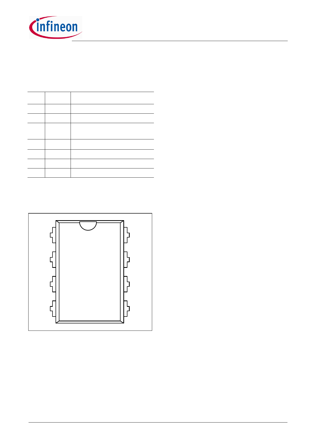
1.1 Pin Configuration with PG-DIP-8 1.3
Pin Functionality
Pin Symbol Function
1 ZC
2 FB
3 CS
4, 5 Drain
6 n.c.
7 VCC
8 GND
1) at Tj=110°C
Zero Crossing
Feedback
Current Sense/
650V1) CoolMOS® Source
650V1) CoolMOS® Drain
Not connected
Controller Supply Voltage
Controller Ground
1.2 Package PG-DIP-8
ZC (Zero Crossing)
At this pin, the voltage from the auxiliary winding after
a time delay circuit is applied. Internally, this pin is
connected to the zero-crossing detector for switch-on
determination. Additionally, the output overvoltage
detection is realized by comparing the voltage Vzc with
an internal preset threshold.
FB (Feedback)
Normally, an external capacitor is connected to this pin
for a smooth voltage VFB. Internally, this pin is
connected to the PWM signal generator for switch-off
determination (together with the current sensing
signal), the digital signal processing for the frequency
reduction with decreasing load during normal
operation, and the Active Burst Mode controller for
entering Active Burst Mode operation determination
and burst ratio control during Active Burst Mode
operation. Additionally, the open-loop / over-load
protection is implemented by monitoring the voltage at
this pin.
ZC 1
FB 2
CS 3
CS (Current Sense)
8
GND
This pin is connected to the shunt resistor for the
primary current sensing, externally, and the PWM
signal generator for switch-off determination (together
with the feedback voltage), internally. Moreover, short-
7
VCC
winding protection is realised by monitoring the voltage
Vcs during on-time of the main power switch.
Drain (Drain of integrated Depl. CoolMOS®)
6
n.c.
Drain pin is the connection to the drain of the internal
CoolMOS®.
Drain
4
5 Drain
Figure 1 Pin Configuration PG-DIP-8 (top view)
Note: Pin 4 and 5 are shorted
VCC (Power supply)
VCC pin is the positive supply of the IC. The operating
range is between VVCCoff and VVCCOVP.
GND (Ground)
This is the common ground of the controller.
Version 2.5
5 July 4, 2011
http://www.Datasheet4U.com
5 Page 
CoolSET® - Q1
ICE2QR0665
Functional Description
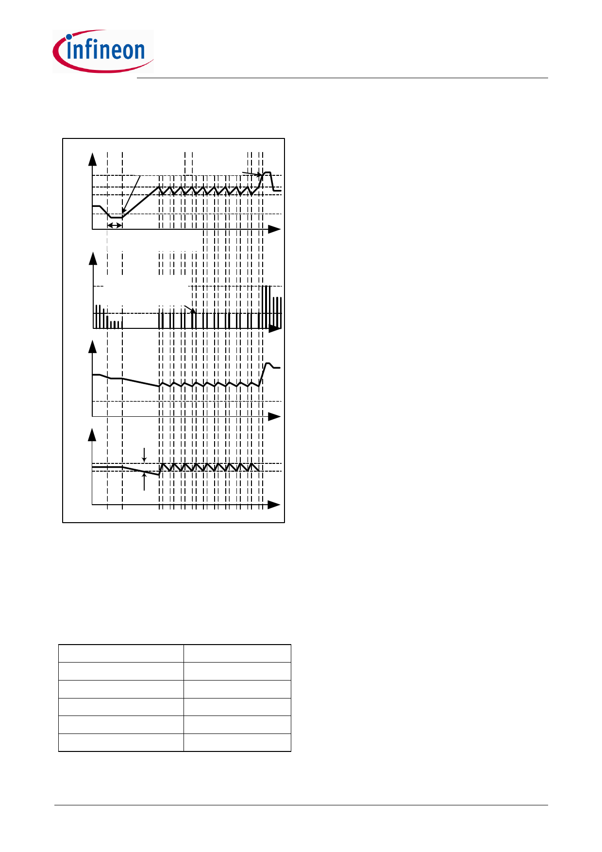
immediately after leaving Active Burst Mode. This is
helpful to decrease the output voltage undershoot.
VFB
VFBLB
VFBBOn
VFBBOff
Entering
Active Burst
Mode
Leaving
Active Burst
Mode
VFBEB
VCS
Time to 7th zero and
Blanking Window (tBEB)
t
1.0V
VCSB
VVCC
Current limit level
during Active Burst
Mode
t
VVCCoff
VO
Max. Ripple < 1%
t
IC is reset and the main power switch is then kept off.
After the VCC voltage falls below the threshold VVCCoff,
the startup cell is activated. The VCC capacitor is then
charged up. Once the voltage exceeds the threshold
VVCCon, the IC begins to operate with a new soft-start.
In case of open control loop or output over load, the
feedback voltage will be pulled up . After a blanking
time of 24ms, the IC enters auto-restart mode. The
blanking time here enables the converter to provide a
high power in case the increase in VFB is due to a
sudden load increase. During off-time of the power
switch, the voltage at the zero-crossing pin is
monitored for output over-voltage detection. If the
voltage is higher than the preset threshold vZCOVP, the
IC is latched off after the preset blanking time.
If the junction temperature of IC exceeds 140 ×C, the
IC enter into autorestart mode.
If the voltage at the current sensing pin is higher than
the preset threshold vCSSW during on-time of the power
switch, the IC is latched off. This is short-winding
protection.
During latch-off protection mode, when the VCC
voltage drops to 10.5V,the startup cell is activated and
the VCC voltage is charged to 18V then the startup cell
is shut down again and repeats the previous procedure.
There is also an maximum on time limitation inside
ICE2QR0665. Once the gate voltage is high longer
than tOnMAx, it is turned off immediately.
Figure 8 Signals in Active Burst Mode
t
3.6 Protection Functions
The IC provides full protection functions. The following
table summarizes these protection functions.
Table 2 Protection features
VCC Overvoltage
Auto Restart Mode
VCC Undervoltage
Auto Restart Mode
Overload/Open Loop
Auto Restart Mode
Over temperature
Auto Restart Mode
Output Overvoltage
Latched Off Mode
Short Winding
Latched Off Mode
During operation, the VCC voltage is continuously
monitored. In case of an under- or an over-voltage, the
Version 2.5
11
July 4, 2011
http://www.Datasheet4U.com
11 Page | ||
| Páginas | Total 21 Páginas | |
| PDF Descargar | [ Datasheet ICE2QR0665.PDF ] | |
Hoja de datos destacado
| Número de pieza | Descripción | Fabricantes |
| ICE2QR0665 | Off-Line SMPS Quasi-Resonant PWM Controller | Infineon Technologies |
| ICE2QR0665G | Off-Line SMPS Quasi-Resonant PWM Controller | Infineon Technologies |
| ICE2QR0665Z | Off-Line SMPS Quasi-Resonant PWM Controller | Infineon Technologies |
| Número de pieza | Descripción | Fabricantes |
| SLA6805M | High Voltage 3 phase Motor Driver IC. |
Sanken |
| SDC1742 | 12- and 14-Bit Hybrid Synchro / Resolver-to-Digital Converters. |
Analog Devices |
|
DataSheet.es es una pagina web que funciona como un repositorio de manuales o hoja de datos de muchos de los productos más populares, |
| DataSheet.es | 2020 | Privacy Policy | Contacto | Buscar |
