|
|
|
PDF HCPL-0720 Data sheet ( Hoja de datos )
| Número de pieza | HCPL-0720 | |
| Descripción | CMOS Optocoupler | |
| Fabricantes | Agilent | |
| Logotipo | ||
Hay una vista previa y un enlace de descarga de HCPL-0720 (archivo pdf) en la parte inferior de esta página. Total 18 Páginas | ||
|
No Preview Available !
Agilent
HCPL-0720/7720 and HCPL-0721/7721
40 ns Propagation Delay,
CMOS Optocoupler
Data Sheet
Description
Available in either an 8-pin DIP or
SO-8 package style respectively, the
HCPL-772X or HCPL-072X
optocouplers utilize the latest
CMOS IC technology to achieve
outstanding performance with very
low power consumption. The
HCPL-772X/072X require only two
bypass capacitors for complete
CMOS compatability.
Basic building blocks of the
HCPL-772X/072X are a CMOS
LED driver IC, a high speed LED
and a CMOS detector IC. A CMOS
logic input signal controls the
LED driver IC which supplies
current to the LED. The detector
IC incorporates an integrated
photodiode, a high-speed
transimpedance amplifier, and a
voltage comparator with an
output driver.
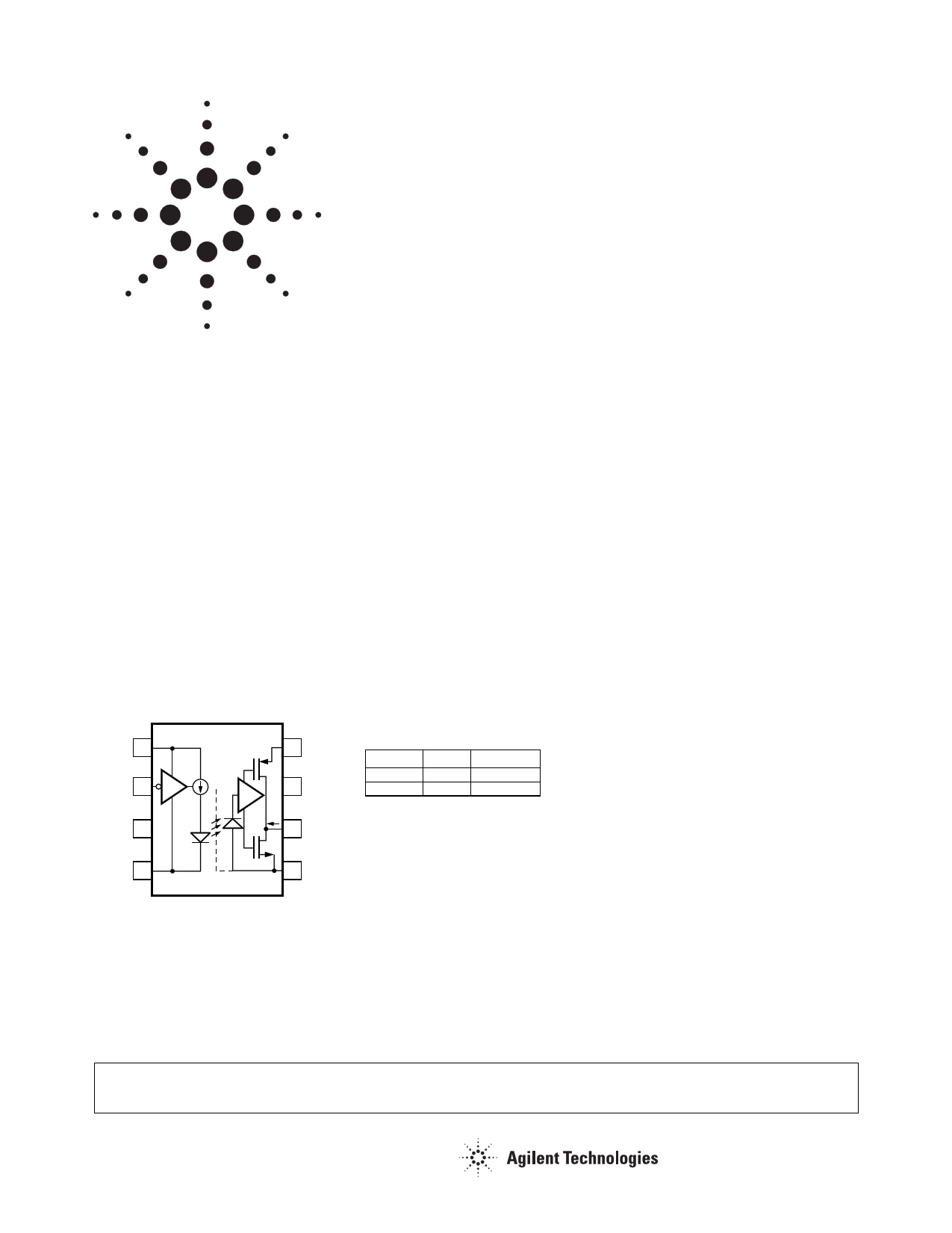
Functional Diagram
**VDD1 1
VI 2
*3
GND1 4
LED1
SHIELD
8 VDD2**
7 NC*
IO
6 VO
5 GND2
TRUTH TABLE
(POSITIVE LOGIC)
VI, INPUT
H
L
LED1
OFF
ON
VO, OUTPUT
H
L
* Pin 3 is the anode of the internal LED and must be left unconnected for
guaranteed data sheet performance. Pin 7 is not connected internally.
**A 0.1 µF bypass capacitor must be connected between pins 1 and 4, and
5 and 8.
Features
• +5 V CMOS compatibility
• 20 ns maximum prop. delay skew
• High speed: 25 MBd
• 40 ns max. prop. delay
• 10 kV/µs minimum common mode
rejection
• –40 to 85°C temperature range
• Safety and regulatory approvals
UL recognized
3750 V rms for 1 min. per
UL 1577
CSA component acceptance
notice #5
IEC/EN/DIN EN 60747-5-2
– VIORM = 630 Vpeak for
HCPL-772X option 060
– VIORM = 560 Vpeak for
HCPL-072X option 060
Applications
• Digital fieldbus isolation: CC-Link,
DeviceNet, Profibus, SDS
• AC plasma display panel level
shifting
• Multiplexed data transmission
• Computer peripheral interface
• Microprocessor system interface
CAUTION: It is advised that normal static precautions be taken in handling and assembly of this
component to prevent damage and/or degradation which may be induced by ESD.
Free Datasheet http://www.Datasheet4U.com
1 page 
Insulation and Safety Related Specifications
Value
Parameter
Symbol 772X 072X
Minimum External Air
Gap (Clearance)
L(I01) 7.1
4.9
Minimum External
Tracking (Creepage)
L(I02) 7.4
4.8
Minimum Internal Plastic
Gap (Internal Clearance)
0.08 0.08
Tracking Resistance
CTI ≥175 ≥175
(Comparative Tracking
Index)
Isolation Group
IIIa IIIa
Units
mm
mm
mm
Volts
Conditions
Measured from input terminals to output
terminals, shortest distance through air.
Measured from input terminals to output
terminals, shortest distance path along body.
Insulation thickness between emitter and
detector; also known as distance through
insulation.
DIN IEC 112/VDE 0303 Part 1
Material Group (DIN VDE 0110, 1/89,
Table 1)
All Agilent data sheets report the
creepage and clearance inherent
to the optocoupler component
itself. These dimensions are
needed as a starting point for the
equipment designer when
determining the circuit insulation
requirements. However, once
mounted on a printed circuit
board, minimum creepage and
clearance requirements must be
met as specified for individual
equipment standards. For
creepage, the shortest distance
path along the surface of a
printed circuit board between the
solder fillets of the input and
output leads must be considered.
There are recommended
techniques such as grooves and
ribs which may be used on a
printed circuit board to achieve
desired creepage and clearances.
Creepage and clearance distances
will also change depending on
factors such as pollution degree
and insulation level.
5
Free Datasheet http://www.Datasheet4U.com
5 Page 
Pulse-width distortion (PWD) is
the difference between tPHL and
tPLH and often determines the
maximum data rate capability of a
transmission system. PWD can be
expressed in percent by dividing
the PWD (in ns) by the minimum
pulse width (in ns) being trans-
mitted. Typically, PWD on the
order of 20 - 30% of the minimum
pulse width is tolerable.
Propagation delay skew, tPSK, is
an important parameter to con-
sider in parallel data applications
where synchronization of signals
on parallel data lines is a concern.
If the parallel data is being sent
through a group of optocouplers,
differences in propagation delays
will cause the data to arrive at the
outputs of the optocouplers at
different times. If this difference
in propagation delay is large
enough it will determine the
maximum rate at which parallel
data can be sent through the
optocouplers.
Propagation delay skew is defined
as the difference between the
minimum and maximum propa-
gation delays, either tPLH or tPHL,
for any given group of optocoup-
lers which are operating under
the same conditions (i.e., the same
drive current, supply voltage,
output load, and operating
temperature). As illustrated in
Figure 13, if the inputs of a group
of optocouplers are switched
either ON or OFF at the same
time, tPSK is the difference
between the shortest propagation
delay, either tPLH or tPHL, and the
longest propagation delay, either
tPLH or tPHL.
As mentioned earlier, tPSK can
determine the maximum parallel
data transmission rate. Figure 14
is the timing diagram of a typical
parallel data application with
both the clock and data lines
being sent through the
optocouplers. The figure shows
data and clock signals at the
inputs and outputs of the
optocouplers. In this case the data
is assumed to be clocked off of the
rising edge of the clock.
VI 50%
VO
2.5 V,
CMOS
tPSK
VI 50%
VO
2.5 V,
CMOS
Figure 13. Propagation delay skew waveform.
DATA
INPUTS
CLOCK
DATA
OUTPUTS
CLOCK
tPSK
tPSK
Figure 14. Parallel data transmission example.
Propagation delay skew repre-
sents the uncertainty of where an
edge might be after being sent
through an optocoupler. Figure 14
shows that there will be
uncertainty in both the data and
clock lines. It is important that
these two areas of uncertainty not
overlap, otherwise the clock
signal might arrive before all of
the data outputs have settled, or
some of the data outputs may
start to change before the clock
signal has arrived. From these
considerations, the absolute
minimum pulse width that can be
sent through optocouplers in a
parallel application is twice tPSK.
A cautious design should use a
slightly longer pulse width to
ensure that any additional
uncertainty in the rest of the
circuit does not cause a problem.
The HCPL-772X/072X
optocouplers offer the advantage
of guaranteed specifications for
propagation delays, pulse-width
distortion, and propagation delay
skew over the recommended
temperature and power supply
ranges.
11
Free Datasheet http://www.Datasheet4U.com
11 Page | ||
| Páginas | Total 18 Páginas | |
| PDF Descargar | [ Datasheet HCPL-0720.PDF ] | |
Hoja de datos destacado
| Número de pieza | Descripción | Fabricantes |
| HCPL-0720 | CMOS Optocoupler | Agilent |
| HCPL-0720 | CMOS Optocoupler | Avago |
| HCPL-0721 | CMOS Optocoupler | Agilent |
| HCPL-0721 | CMOS Optocoupler | Avago |
| Número de pieza | Descripción | Fabricantes |
| SLA6805M | High Voltage 3 phase Motor Driver IC. |
Sanken |
| SDC1742 | 12- and 14-Bit Hybrid Synchro / Resolver-to-Digital Converters. |
Analog Devices |
|
DataSheet.es es una pagina web que funciona como un repositorio de manuales o hoja de datos de muchos de los productos más populares, |
| DataSheet.es | 2020 | Privacy Policy | Contacto | Buscar |