No Preview Available !

Product Information
STR-W6700 Series Off-Line
Quasi-Resonant Switching Regulators
Introduction
The Series STR-W6750 devices are hybrid integrated cir-
cuits (HICs) with a built-in power MOSFET and a control
IC designed for quasi-resonant type switch-mode power
supplies (SMPS). In normal operation, the HIC provides
high efficiency and low EMI noise with bottom-skip quasi-
resonant operation during light output loads. Low power
consumption is also achieved by blocking (intermittent)
oscillation during an auto-burst mode and reduced even
further in a manually triggered (clamping an output voltage)
standby mode.
The HIC is supplied in a seven-pin fully-molded TO-220-
style package with pin 2 deleted, which is suitable for down-
sizingand standardizing of an SMPS by reducing external
componentcount and simplifying circuit design.
Features and benefits include the following:
▪ Blocking (or intermittent) oscillation operation by
reducing output voltage in the standby mode.
▪ In addition to the standard quasi-resonant operation, a
bottom-skip function is available for increased efficiency
from light to medium load.
▪ Soft-start operation at start-up.
▪ Reduced switching noise (compared to conventional
PWM hard-switching solution) with a step-drive
function.
▪ Built-in avalanche-energy-guaranteed power MOSFET
(to simplify surge-absorption circuit; no VDSS derating
is required).
▪ Overcurrent protection (OCP), overvoltage protection
(OVP), overload protection (OLP), and maximum
ON-time control circuits are incorporated. OVP and OLP
go into a latched mode.
▪ Able to save SMPS design time with present designs and
evaluation processes.
Figure 1. STR-W6700 series packages are fully molded TO-220
package types. Pin 2 is deleted for greater isolation.
Table 1. Product Line-up
Type #
STR-W6735
MOSFET
VDSS
(V)
500
RDS(on)
(Max)
(Ω)
0.57
VAC
Input
(V)
120
POUT*
(W)
160
STR-W6753
Wide
1.70
230
58
120
STR-W6754
650
Wide
0.96
230
100
160
STR-W6756
Wide
0.73
230
140
240
STR-W6765
800
Wide
1.80
230
50
110
*The listed output power represents thermal ratings, and the peak
output power, POUT , is obtained by 120% to 140% of the thermal
rating value. In case of low output voltage and narrow on-duty
cycle, the POUT (W) becomes lower than the above.
Contents
Introduction
Pin functional descriptions
Operation description
Transformer parameters
General considerations
Design considerations
Package Dimensions, TO-220
Worldwide Contacts
28103.30
1
2
6
10 All performance characteristics given are typical values for
11 circuit or system baseline design only and are at the nominal
13 operating voltage and an ambient temperature of 25°C, un-
14 less otherwise stated.
17
SANKEN ELECTRIC CO., LTD.
http://www.sanken-ele.co.jp/en/
Free Datasheet http://www.Datasheet4U.com
1 page


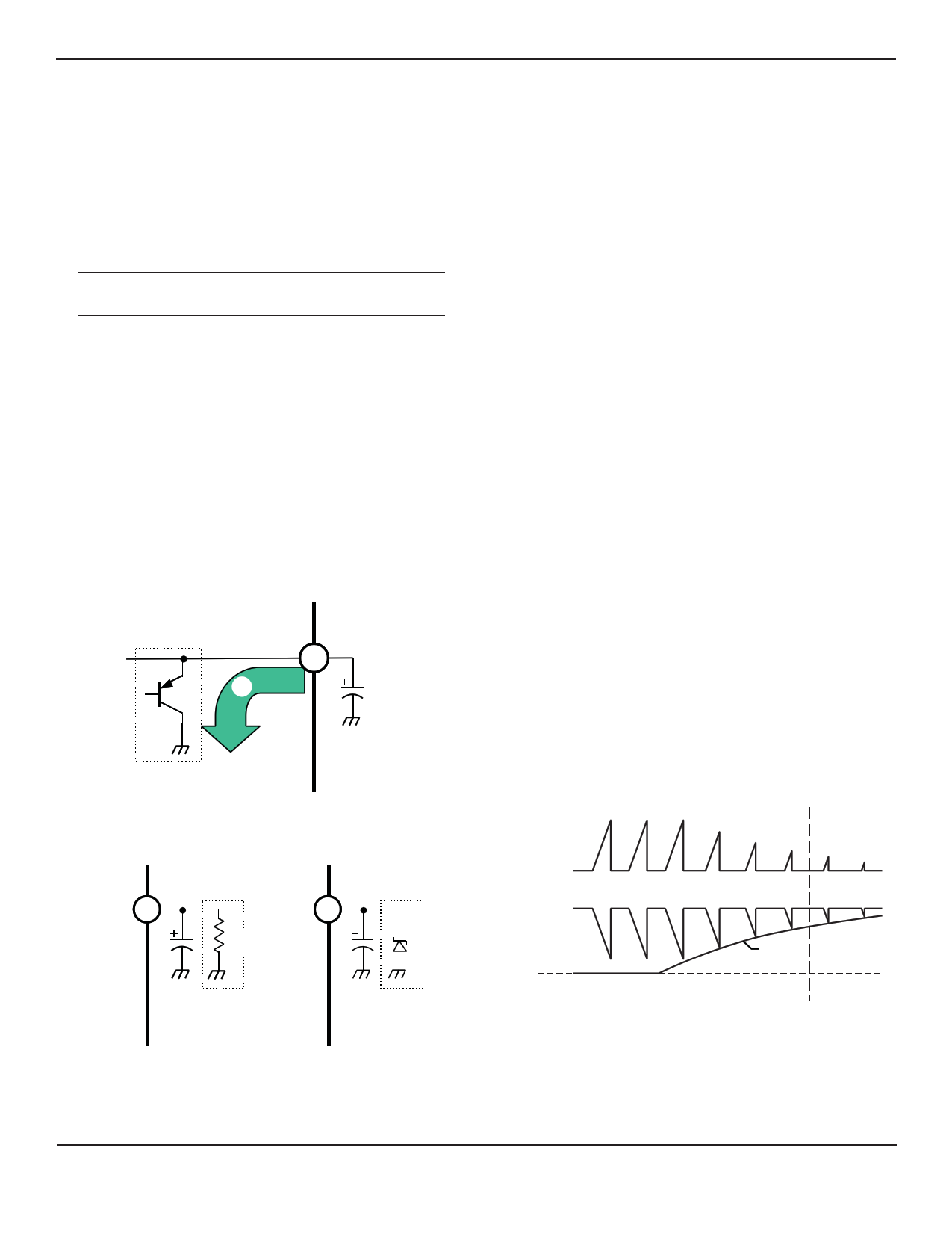
In the overload mode, where drain current is controlled by OCP
operation, the secondary-side output voltage drops. Accordingly,
the error-amplifier and photocoupler on the secondary side are
cut off. The STR-W6700 series regards the signal absence with
continuous OCP operation as an overload status, and the SS/OLP
pin voltage starts rising by ISSOLP(OLP) as shown in figure 10 and
in the following table:
OLP timing (0 to 4.9 V, charging current: 11 μA)
CSS (μF) 0.47
1.0
2.2
3.3
4.7
Time (ms) 209 445 980 1470 2094
NOTE: A large CSS value also results in a longer soft-start time.
After the SS/OLP pin voltage keeps rising to the OLP-Operation
Threshold Voltage (VSSOLP(OLP) = 4.9 V), the oscillation stops,
and the IC goes into a latched mode.
The time from OLP activation to a latched mode should be
obtained from the following formula, assuming ISSOLP(OLP) is
from a constant-current circuit:
t = CSS × ∆V
ISSOLP(OLP)
(2)
where ∆V is the capacitor charging voltage of approximately 4.9 V.
However, the ISSOLP(OLP) is dependent on the SS/OLP pin voltage,
and ISSOLP(OLP) drops as the SS/OLP pin voltage rises. The actual
SS/OLP
5
V
CSS
current value therefore does not exactly match the value calcu-
lated in the equation above, and the actual load conditions should
be carefully considered. Also, make sure that OCP operation at
power supply start-up does NOT place the IC in a latched mode.
Note: During this period, if VCC goes below the UVLO thresh-
old voltage, the IC does not go into a latch mode, but goes into
intermittent operation. Where the CSS voltage rises to 4.9 V and
VCC does not go below the UVLO threshold voltage, the IC goes
into a latched mode.
Operation at power supply turn off At power supply turn
off, voltage on capacitor CSS, which is externally connected to
the SS/OLP pin, is discharged by way of an internal RESET cir-
cuit as shown in figure 11. The RESET circuit does not operate in
normal operation while the internal regulator circuit operates.
Deactivating the OLP circuit To deactivate the OLP circuit
while soft-start is active, connect either a 47 kΩ resistor or a
Zener diode to the SS/OLP pin (figure 12). By doing this, OLP
operation is deactivated at start-up or during an overload status.
FB (Pin 6)
The FB pin is used in either a normal mode (constant-voltage-
control circuit operation) or in a standby mode. Refer to Standby
Operation section for controlling in the standby mode.
Constant voltage control circuit The STR-W6700 series
adopts the current-mode control circuit, which ensures stability
with a heavy load. The peak value of the MOSFET drain current
(at on-time) is changed by comparing the FB pin voltage with the
internal VOCPM. Off-time becomes quasi-resonant operation syn-
chronized to the reset signal from a transformer. Where no reset
signal is input from the transformer, it becomes fixed oscillation
frequency (approximately 22 kHz) set by the internal oscillator
Figure 11. Reset circuit at power turn off
SS/OLP
5
SS/OLP
5
47 kΩ
IDS
GND
VOCPM
VOCPD(LIM)
GND
Overload
VFB
Normal Load
Light Load
Figure 12. OLP deactivation circuit alternative configurations
Figure 13. Constant-voltage control at fixed oscillation frequency (quasi-
resonant signal not available)
STRY6700-AN Rev. 2.0
SANKEN ELECTRIC CO., LTD.
5
Free Datasheet http://www.Datasheet4U.com
5 Page


In addition, in the design of the transformer, using 130% of the
estimated peak switching current is recommended to ensure that
the transformer is not saturated, based on the plot of N × I-limit
(AT) versus AL-value (nH / N2).
Instead of performing the calculations above, software that pro-
vides a complete flyback transformer design tool is available.
CRT TV application concerns:
• Rather than winding with a single thick wire, a thin and
bifilar or trifilar winding across the entire width of bobbin is
recommended.
• For windings where NP and +B are a large number of turns,
divisional sandwich winding is recommended.
• For an output where a tight regulation is required, winding
with good coupling with S1 (+B) is recommended.
• For the +B winding, better coupling by use of litz wire is
required. In case the litz wire does not fit into a the bobbin
winding width, reduce the wire size, and use 2 to 3 of them in
strands.
• For improved thermal design:
▫ Leakage flux of wires close to the core center becomes large.
Eddy current can be reduced by the use of litz wire.
▫ In case the entire winding does not fit into the available
winding thickness, reduce the size of wires from outer side.
▫ Wire diameter is determined based on actual current and
should be less than 4 A / mm2.
Single and/or low-voltage output concerns:
• Wind so that wires are parallel and with good coupling.
• Sandwich winding is recommended.
General considerations
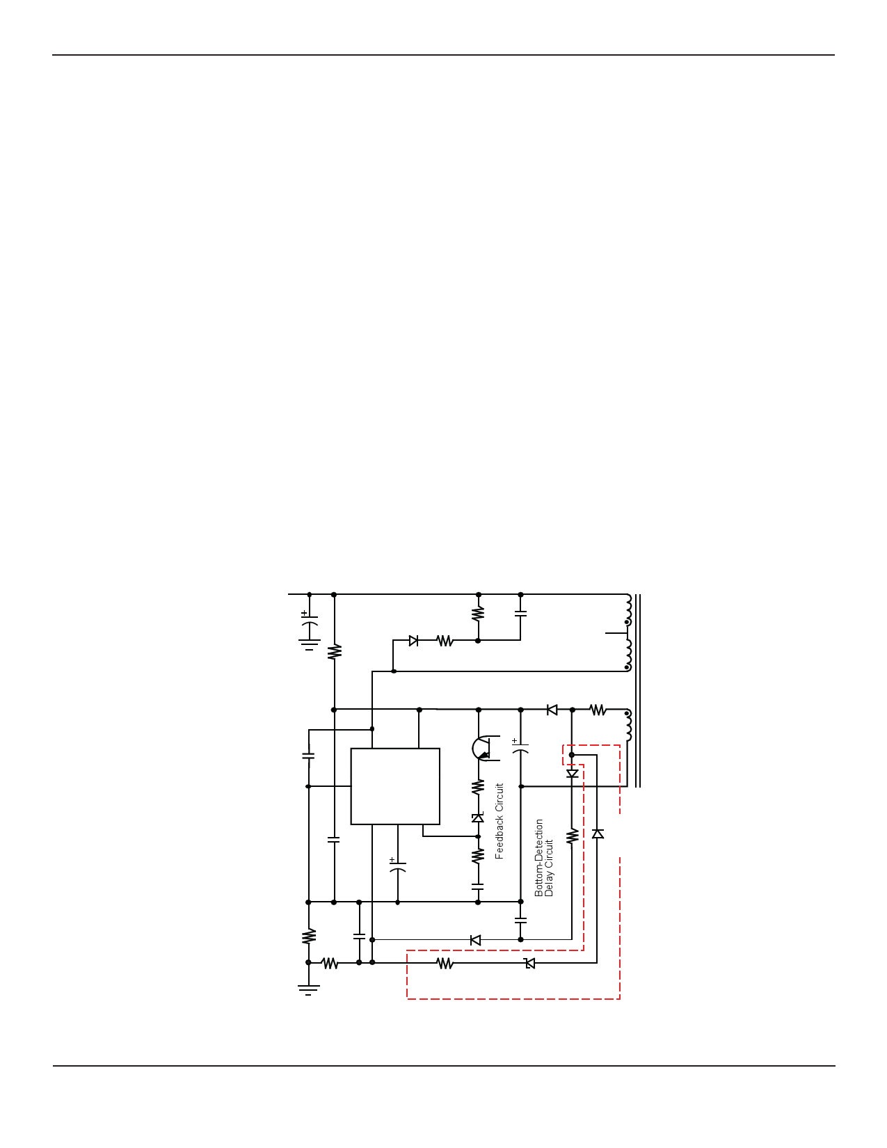
Universal AC input correction in OCP
With a universal AC input application, as described in the
Overload Protection (OLP) section, the load conditions for OCP
activation vary according to input voltage level, 110 V or 230 V.
Figure 23 illustrates a solution.
In the loop surrounded by the dashed line, the negative voltage of
the bias winding, which is in proportion to the input voltage level
when the MOSFET switches on, works for the input correction
during OLP.
The Zener diode is set to be on with a 230 VAC input, but not to
be activated with a 110 VAC input. When the bias winding output
voltage is 18 V, the resistor, Zener, and diode within the dashed
line are recommended.
STRY6700-AN Rev. 2.0
Input
Smoothing
Capacitor
Start-up
Resistor
Snubber Circuit
P
P
CVoRltage
Resonant
Capacitor
D VCC
STR-W6700
S/GND
OCP SS/
/BD OLP FB
Bias
D
200 V
Fast
Recovery
Diode
Current-
Sense
Resistor
OCP
Sense
Filter
Bottom-Detection
Delay Circuit
10 to 22 kΩ
16 V
Loop for OCP Matching to Input Voltage
Figure 23. Reference circuit for general application considerations
SANKEN ELECTRIC CO., LTD.
11
Free Datasheet http://www.Datasheet4U.com
11 Page
| 


