|
|
|
PDF XC9248 Data sheet ( Hoja de datos )
| Número de pieza | XC9248 | |
| Descripción | 18V Driver Transistor Built-In Synchronous Step-Down DC/DC Converter | |
| Fabricantes | Torex Semiconductor | |
| Logotipo | ||
Hay una vista previa y un enlace de descarga de XC9248 (archivo pdf) en la parte inferior de esta página. Total 21 Páginas | ||
|
No Preview Available !
XC9248 Series
ETR05022-004
18V Driver Transistor Built-In Synchronous Step-Down DC/DC Converter
GENERAL DESCRIPTION
The XC9248 series is 18V bootstrap synchronous step-down DC/DC converter with built-in Nch-Nch driver transistors.
With an input voltage range from 4.5V to 18V and a maximum output current of 2.2A, the series is suitable for digital home
appliance power supplies and can be used with small ceramic capacitors.
The series has a 0.8V reference voltage, and using externally connected resistors, the output voltage can be set freely from
1.0V to 12V.
The control method is synchronous PWM (Source/ Sink). The soft start time is internally set to 2.8ms (TYP.), also can be
adjusted using external capacitor.
With UVLO (Under Voltage Lock Out) function, the internal driver transistors are forced OFF when input voltage falls down
below 3.8V (TYP.).
The series includes over current protection, VOUT short-circuit protection, Lx short-circuit protection, VOUT overvoltage
protection and thermal shutdown.
APPLICATIONS
Digital home appliance
Office automation equipment
Notebook computers
Car accessories power supplies
FEATURES
Input Voltage
Output Voltage
Output Current
Efficiency
Oscillation Frequency
: 4.5V ~ 18V
: 1.0V~12V (VFB=0.8V±1.5%) (*1)
: 2.2A
: 93.8% (*1) @VIN=12V,VOUT=5V, IOUT=700mA
: 500kHz
Maximum Duty Cycle
: 79%
Soft-Start Time
: Fixed2.8ms, set by external capacitor
Protection Circuit
http://www.DataSheet4U.net/
: UVLO
High side over current protection
Low side over current protection
VOUT Short-circuit Protection
LX Short-circuit Protection
VOUT Over voltage protection
Thermal shutdown
Package
: SOP-8FD
Environmentally Friendly : EU RoHS Compliant, Pb Free
(*1) Performance depends on external components and wiring on the PCB.
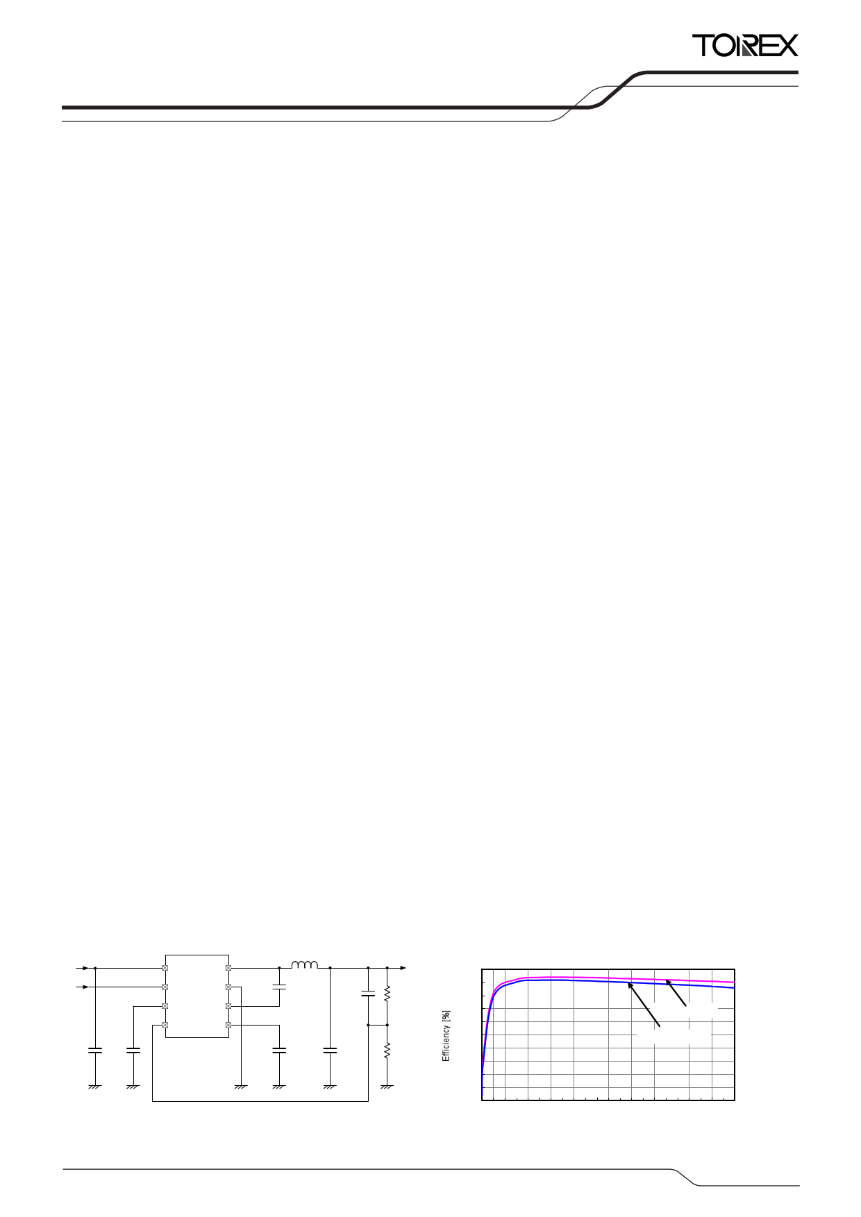
TYPICAL APPLICATION CIRCUIT
TYPICAL PERFORMANCE
CHARACTERISTICS
VIN
EN
CIN CSS
VIN LX
EN GND CBST
SS BST
FB VL
CVL
L
CFB
CL
VOUT
RFB1
RFB2
Efficiency vs. Output Current
100
90
80
70
60
50
40
30
20
10
0
0
Ta=25°C
VIN=12V , VOUT=5V
VIN=12V , VOUT=3.3V
500
1000
1500
Output Current : IOUT [mA]
2000
1/21
datasheet pdf - http://www.DataSheet4U.net/
1 page 
XC9248
Series
ELECTRICAL CHARACTERISTICS
XC9248 Series
PARAMETER
SYMBOL
CONDITIONS
MIN.
TYP.
Ta=25
MAX. UNITS CIRCUIT
Operating Voltage Range
FB Voltage
FB Voltage
Temperature Characteristics
Maximum Output Current
Supply Current
Stand-by Current
Oscillation Frequency
Maximum Duty Cycle
UVLO Detection Voltage
UVLO Release Voltage
Low side Current Limit
Integral Latch Time
(Type A)
Internal Soft-start Time
SS Terminal Current
SS Threshold Voltage
OVP Detection Voltage
Efficiency
Lx SW ”H” ON Resistance
Lx SW ”L” ON Resistance
EN ”H” Voltage
EN ”L” Voltage
LX ”L” Current
EN ”H” Current
EN ”L” Current
FB ”H” Current
FB ”L” Current
Thermal Shutdown Temperature
Hysteresis Width
CL Discharge Resistance
CL Discharge Current
VIN
VFB
VFB/
(VFB・ΔTopr)
IOUTMAX
Iq
ISTB
fOSC
Dmax
VUVLOD
VUVLOR
ILIMLS
tLAT
tSS
ISS
VSSTH
VOVPD
EFFI (*3)
RLXH
RLXL
VENH
VENL
ILXL
IENH
IENL
IFBH
IFBL
TTSD
THYS
RDCHG
IDCHG
When connected to external components
VIN ≦7V: Setup VOUT=3.3V
VIN >7V: Setup VOUT=5V
VFB=Sweep (0.812V→0.788V), VSS=OPEN
-40℃≦Topr≦105℃
When connected to external components
VIN=VEN=18V, VFB=0.9V
VIN=18V, VEN=0V, VFB=OPEN
VFB=0.7V, VSS=OPEN
VFB=0.7V, VSS=OPEN
VIN=Sweep (4.5V→3.5V) , VEN=2V, VFB=0.9V
Voltage when VL pin changes from
“H” level to “L” level (*2)
VIN=Sweep (3.5V→4.5V), VEN=2V, VFB=0.9V
Voltage when VL pin changes from
“L” level to “H” level (*2)
VOUT=4.5V (Forced), Bottom point of LX pin current
VFB=0.9V, ILX = ILIMLS
Time until SS pin changes from
“H” level to “L” level (*2)
VIN=12V, VEN=2V, VFB=0.72V, VSS=OPEN
Time until LX pin oscillates
VSS=0V, VLX=VFB=OPEN
VFB=0.72V, VSS=OPEN
http://www.DataSheet4U.net/
Voltage when LX pin oscillates
VFB=Sweep (0.788V→1.2V), VSS=OPEN
Setup VOUT=5V, IOUT=0.7A
When connected to external components
VIN=12V, VFB=0.9V, VEN=Sweep (0.2V→1.4V)
Voltage when VL pin changes from
“L” level to “H” level (*2)
VIN=12V, VFB=0.9V, VEN=Sweep (1.4V→0.2V)
Voltage when VL pin changes from
“H” level to “L” level (*2)
VIN=18V , VEN=VLX=0V , VFB=VSS=OPEN
VIN=VEN=18V , VLX=VFB=VSS=OPEN
VIN=18V , VEN=0V , VLX=VFB=VSS=OPEN
VIN=18V , VEN=0V , VFB=5V , VLX=VSS=OPEN
VIN=18V , VEN=VFB=0V , VLX=VSS=OPEN
VIN=12V , VEN=0V , VLX=2V , VFB=VSS=OPEN
VIN=12V , VEN=0V , VLX=12V , VFB=VSS=OPEN
4.5 - 18 V
0.788
2.2(*1)
-
-
450
74
0.800
±40
-
0.76
38
500
79
0.812
V
ppm/℃
-A
1.10 mA
51 A
550 kHz
-%
3.50 3.80 4.45
V
3.55 3.90 4.50
2.1 -
-
0.4 1.1 1.8
V
A
ms
- 2.8 -
246
1.2 1.8 2.4
- 0.9 1.2
- 93.8 -
- 0.12(*4) -
- 0.12(*4) -
1.4 -
-
ms
A
V
V
%
Ω
Ω
V
- - 0.2 V
-1 0
-
A
- 16 21
A
-0.1 - 0.1
A
-0.1 - 0.1
A
-0.1 - 0.1
A
- 150 -
°C
- 25 - °C
- 300 -
- 9 - mA
①
②
②
①
③
③
②
②
④
④
⑦
⑤
②
⑥
②
②
⑧
-
-
④
④
-
-
Unless otherwise stated, VIN=VEN=12V
(*1) Mount conditions affect heat dissipation. Maximum output current is not guaranteed when Thermal Shutdown starts to operate earlier.
(*2) “H”=4.3V~5V, “L”=-0.1V~0.1V
(*3) EFFI = {[(output voltage)×(output current)]÷[(input voltage)×(input current)]}×100
(*4) Design value
5/21
datasheet pdf - http://www.DataSheet4U.net/
5 Page 
OPERATIONAL EXPLANATION (Continued)
XC9248
Series
<Thermal Shutdown>
For protection against heat damage of the ICs, thermal shutdown function monitors chip temperature. The thermal shutdown
circuit starts operating and the Nch MOS driver transistor will be turned off when the chip’s temperature reaches 150℃. The LX
pin enters the CL discharged state and stops functioning at GND level (0V). When the temperature drops to 125℃ or less after
shutting of the current flow, the IC performs the soft-start function to initiate output startup operation.
<UVLO Circuit>
When the VIN voltage becomes 3.8V (TYP.) or lower, the Nch MOS driver transistor is forced OFF. The LX pin enters the CL
discharged state and stops functioning at GND level (0V). When the VIN voltage becomes 3.9V (TYP.) or higher, switching
operation takes place. By releasing the UVLO function, the IC performs the soft-start function to initiate output startup operation.
The soft-start function operates even when the VIN voltage falls momentarily below the UVLO detect voltage. The UVLO circuit
does not cause a complete shutdown of the IC, but causes pulse output to be suspended; therefore, the internal circuitry
remains in operation.
<Bootstrap method>
An Nch MOS driver Tr. is used for the High side driver, and a voltage higher than the VIN voltage is needed to turn the driver on.
For that purpose, the bootstrap method is used to generate a voltage higher than the VIN voltage. The CBST capacitance is
connected between BST and LX, and because the VLX voltage is lower than the 4.6V (TYP.) VL voltage that is the internal power
supply, CBST is charged from VL.
<VOUT short-circuit protection>
With the A type, when the output voltage VOUT is shorted to GND or is near a shorted state (the FB voltage is1/2 or lower), and
a current over the current limit flows to the High side or Low side driver Tr., a VOUT short circuit is detected and the High side and
Low side driver Trs. are immediately turned off and latched. The LX pin enters the CL discharged state and stops functioning at
GND level (0V). Once in the latched state, operation is resumed by either turning the IC off and restarting with the EN pin, or by
re-input into the VIN pin (the voltage is lowered below the under-voltage lockout detection voltage once).
<LX short-circuit protection>
If the event that the LX pin shorts to GND, LX short-circuit protection activates for protection from over-current due to rush
current and to protect the IC.
http://www.DataSheet4U.net/
If the LX pin shorts to GND, High side current limiting will activate due to rush current when the High side driver Tr. turns on.
The High side driver Tr. turn offs, and the Low side driver Tr. turns on at the same time. At this time, if Low side current limiting
did not activate, an LX short-circuit is detected, and the Low side driver is turned off and latched at the same time as the High
side driver Tr. Once in the latched state, operation is resumed by either turning the IC off and restarting with the EN pin, or by
re-input into the VIN pin (the voltage is lowered below the under-voltage lockout detection voltage once).
<VOUT over-voltage protection>
To minimize output voltage overshoot, VOUT over-voltage protection activates when VOUT overshoot occurs due to the output
resistance changing from a heavy load to a light load or otherwise. When VOUT overshoot occurs and the FB voltage that senses
VOUT rises to 0.9V (TYP.) or more, the High side driver Tr. is immediately turned off and the Low side driver Tr. is turned on to
prevent VOUT overshoot. When the FB voltage falls to 0.8V (TYP.) or less due to hysteresis, the High side driver Tr. turns on at
the next clock cycle.
11/21
datasheet pdf - http://www.DataSheet4U.net/
11 Page | ||
| Páginas | Total 21 Páginas | |
| PDF Descargar | [ Datasheet XC9248.PDF ] | |
Hoja de datos destacado
| Número de pieza | Descripción | Fabricantes |
| XC9246 | 16V Driver Transistor Built-In Step-Down DC/DC Converters | Torex Semiconductor |
| XC9247 | 16V Driver Transistor Built-In Step-Down DC/DC Converters | Torex Semiconductor |
| XC9248 | 18V Driver Transistor Built-In Synchronous Step-Down DC/DC Converter | Torex Semiconductor |
| Número de pieza | Descripción | Fabricantes |
| SLA6805M | High Voltage 3 phase Motor Driver IC. |
Sanken |
| SDC1742 | 12- and 14-Bit Hybrid Synchro / Resolver-to-Digital Converters. |
Analog Devices |
|
DataSheet.es es una pagina web que funciona como un repositorio de manuales o hoja de datos de muchos de los productos más populares, |
| DataSheet.es | 2020 | Privacy Policy | Contacto | Buscar |