|
|
PDF MAX44248 Data sheet ( Hoja de datos )
| Número de pieza | MAX44248 | |
| Descripción | Dual Op Amp | |
| Fabricantes | Maxim Integrated | |
| Logotipo |  |
|
Hay una vista previa y un enlace de descarga de MAX44248 (archivo pdf) en la parte inferior de esta página. Total 13 Páginas | ||
|
No Preview Available !
EVALUATION KIT AVAILABLE
MAX44248
36V, Precision, Low-Power, 90µA, Dual Op Amp
General Description
The MAX44248 is an ultra-precision, low-noise, zero-drift
dual operational amplifier featuring very low-power oper-
ation with a wide supply range. The device incorporates
a patented auto-zero circuit that constantly measures
and compensates the input offset to eliminate drift over
time and temperature as well as the effect of 1/f noise.
The device also features integrated EMI filters to reduce
high-frequency signal demodulation on the output. The
op amp operates from either a single 2.7V to 36V supply
or dual ±1.35V to ±18V supply. The device is unity-gain
stable with a 1MHz gain-bandwidth product and a low
90µA supply current per amplifier.
The low offset and noise specifications and high supply
range make the device ideal for sensor interfaces and
transmitters.
The device is available in 8-pin FMAXM and SO packages
and is specified over the -40NC to +125NC automotive
operating temperature range.
Applications
Sensors Interfaces
4-20mA and 0 to10V Transmitters
PLC Analog I/O Modules
Weight Scales
Portable Medical Devices
Features
S Very Low Input Voltage Offset 7.5µV (max)
S Low 30nV/NC Offset Drift (max)
S Low 90µA Quiescent Current per Amplifier
S Low Input Noise
50nV/√Hz at 1kHz
0.5µVP-P from 0.1Hz to 10Hz
S 1MHz Gain-Bandwidth Product
S EMI Suppression Circuitry
S Rail-to-Rail Output
S 2.7V to 36V Supply Range
S 8-Pin µMAX and SO package
Ordering Information appears at end of data sheet.
For related parts and recommended products to use with this part,
referwww.DataSheet.net/ to www.maximintegrated.com/MAX44248.related.
µMAX is a registered trademark of Maxim Integrated Products, Inc.
Typical Operating Circuit
MAX6033
REF
MAX5216
DAC
VREF
R1
R2
R3
MAX44248
LP+
ISIG
(4-20mA)
RSENSE
LP-
For pricing, delivery, and ordering information, please contact Maxim Direct
at 1-888-629-4642, or visit Maxim’s website at www.maximintegrated.com.
19-6367; Rev 0; 7/12
Datasheet pdf - http://www.DataSheet4U.co.kr/
1 page 
MAX44248
36V, Precision, Low-Power, 90µA, Dual Op Amp
Typical Operating Characteristics
(TVADD==+2150°VC, ,VuSnSle=ss0Vo,thVeINrw+is=eVnIoNt-e=d.V) DD/2, RL = 5kω to VDD/2. Typical values are at TA = +25°C.)
INPUT OFFSET VOLTAGE HISTOGRAM
45
40
35
30
25
20
15
10
5
0
0 0.5 1.0 1.5 2.0 2.5 3.0 3.5
INPUT OFFSET VOLTAGE (µV)
INPUT OFFSET VOLTAGE DRIFT
35
30
25
20
15
10
5
0
4 5 6 7 8 9 10 11 12 13 14
INPUT OFFSET VOLTAGE DRIFT (nV/°C)
100
98
96
94
92
90
88
86
84
82
80
0
SUPPLY CURRENT
vs. SUPPLY VOLTAGE
10 20 30
SUPPLY VOLTAGE (V)
40
SUPPLY CURRENT
vs. TEMPERATURE
100
98
96
94
92
90
88
86
84
82
80
-50 -25
0 25 50 75 100 125
TEMPERATURE (°C)
INPUT BIAS CURRENT
VS. COMMON-MODE VOLTAGE
180
160
140
120
100
80
60
40
20
0
02468
COMMON-MODE VOLTAGE (V)
2
1
0
-1
-2
-3
-4
-6
10
INPUT OFFSET VOLTAGE
vs. COMMON-MODE VOLTAGE
www.DataSheet.net/
-4 -2 0 2 4
COMMON-MODE VOLTAGE (V)
6
800
INPUT OFFSET VOLTAGE
VS. TEMPERATURE
3
2
1
0
-1
-2
-3
-4
-5
-50 -25
0 25 50 75 100 125
TEMPERATURE (°C)
INPUT BIAS CURRENT
vs. TEMPERATURE
600
400
200
0
-200
-400
-50 -25
0 25 50 75 100 125
TEMPERATURE (°C)
Maxim Integrated
5
Datasheet pdf - http://www.DataSheet4U.co.kr/
5 Page 
MAX44248
36V, Precision, Low-Power, 90µA, Dual Op Amp
Layout Guidelines
The MAX44248 features ultra-low voltage and noise.
Therefore, to get optimum performance follow the layout
guidelines.
Avoid temperature tradients at the junction of two
dissimilar metals. The most common dissimilar metals
used on a PCB are solder-to-component lead and
solder-to-board trace. Dissimilar metals create a local
thermocouple. A variation in temperature across the
board can cause an additional offset due to Seebeck
effect at the solder junctions. To minimize the Seebeck
effect, place the amplifier away from potential heat
sources on the board, if possible. Orient the resistors
such that both the ends are heated equally. It is a good
practice to match the input signal path to ensure that the
type and number of thermoelectric juntions remain the
same. For example, consider using dummy 0ω resistors
oriented in such a way that the thermoelectric source, due
to the real resistors in the signal path, are cancelled. It is
recommended to flood the PCB with ground plane. The
ground plane ensures that heat is distributed uniformly
reducing the potential offset voltage degradation due to
Seebeck effect.
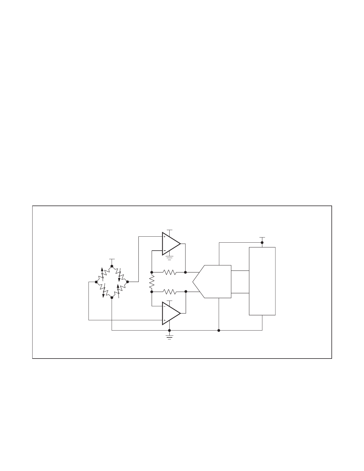
5V
Figure 1. Weight Application
5V
AMP A
MAX44248
www.DataSheet.net/
5V
VDD
RF
RG RF
VDD
VIN+
MAX11205
VIN- VSS
OUTPUT
MICRO
CONTROLLER
AMP B
MAX44248
Maxim Integrated
11
Datasheet pdf - http://www.DataSheet4U.co.kr/
11 Page | ||
| Páginas | Total 13 Páginas | |
| PDF Descargar | [ Datasheet MAX44248.PDF ] | |
Hoja de datos destacado
| Número de pieza | Descripción | Fabricantes |
| MAX44241 | Single/Quad/Dual Op Amps | Maxim Integrated |
| MAX44243 | Single/Quad/Dual Op Amps | Maxim Integrated |
| MAX44244 | Single/Quad/Dual Op Amps | Maxim Integrated |
| MAX44245 | Single/Quad/Dual Op Amps | Maxim Integrated |
| Número de pieza | Descripción | Fabricantes |
| SLA6805M | High Voltage 3 phase Motor Driver IC. |
Sanken |
| SDC1742 | 12- and 14-Bit Hybrid Synchro / Resolver-to-Digital Converters. |
Analog Devices |
|
DataSheet.es es una pagina web que funciona como un repositorio de manuales o hoja de datos de muchos de los productos más populares, |
| DataSheet.es | 2020 | Privacy Policy | Contacto | Buscar |
