|
|
|
PDF AD5700 Data sheet ( Hoja de datos )
| Número de pieza | AD5700 | |
| Descripción | Low Power HART Modem | |
| Fabricantes | Analog Devices | |
| Logotipo | ||
1. AD5700 Hay una vista previa y un enlace de descarga de AD5700 (archivo pdf) en la parte inferior de esta página. Total 20 Páginas | ||
|
No Preview Available !
www.DataSheet.co.kr
Data Sheet
Low Power HART Modem
AD5700/AD5700-1
FEATURES
GENERAL DESCRIPTION
HART-compliant fully integrated FSK modem
1200 Hz and 2200 Hz sinusoidal shift frequencies
115 μA maximum supply current in receive mode
Suitable for intrinsically safe applications
Integrated receive band-pass filter
Minimal external components required
Clocking optimized for various system configurations
Ultralow power crystal oscillator (60 μA maximum)
External CMOS clock source
Precision internal oscillator (AD5700-1 only)
Buffered HART output—extra drive capability
8 kV HBM ESD rating
2 V to 5.5 V power supply
1.71 V to 5.5 V interface
−40°C to +125°C operation
4 mm × 4 mm LFCSP package
HART physical layer compliant
UART interface
APPLICATIONS
Field transmitters
HART multiplexers
PLC and DCS analog I/O modules
HART network connectivity
The AD5700/AD5700-1 are single-chip solutions, designed
and specified to operate as a HART® FSK half-duplex modem,
complying with the HART physical layer requirements. The
AD5700/AD5700-1 integrate all of the necessary filtering, signal
detection, modulating, demodulating and signal generation
functions, thus requiring few external components. The 0.5%
precision internal oscillator on the AD5700-1 greatly reduces
the board space requirements, making it ideal for line-powered
applications in both master and slave configurations. The maxi-
mum supply current consumption is 115 μA, making the AD5700/
AD5700-1 an optimal choice for low power loop-powered applica-
tions. Transmit waveforms are phase continuous 1200 Hz and
2200 Hz sinusoids. The AD5700/AD5700-1 contain accurate
carrier detect circuitry and use a standard UART interface.
Table 1. Related Products
Part No. Description
AD5755-1
Quad-channel, 16-bit, serial input, 4 mA to 20 mA and
voltage output DAC, dynamic power control, HART
connectivity
AD5421 16-bit, serial input, loop powered, 4 mA to 20 mA DAC
AD5410/
AD5420
Single-channel, 12-bit/16-bit, serial input, 4 mA to 20 mA
current source DACs
AD5412/
AD5422
Single-channel, 12-bit/16-bit, serial input, current
source and voltage output DACs
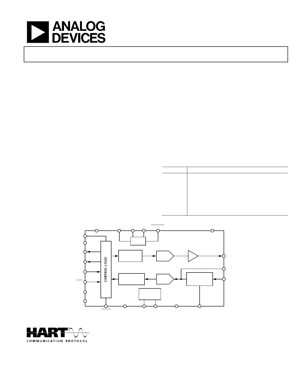
FUNCTIONAL BLOCK DIAGRAM
REG_CAP
CLKOUT XTAL1 XTAL2 XTAL_EN
VCC
IOVCC
DUPLEX
CD
RXD
TXD
RTS
OSC
FSK
MODULATOR
FSK
DEMODULATOR
AD5700/AD5700-1
DAC
BUFFER
ADC
BAND-PASS
FILTER AND
BIASING
HART_OUT
ADC_IP
HART_IN
CLK_CFG0
CLK_CFG1
VOLTAGE
REFERENCE
RESET
DGND
REF REF_EN
Figure 1.
AGND
FILTER_SEL
Rev. 0
Information furnished by Analog Devices is believed to be accurate and reliable. However, no
responsibility is assumed by Analog Devices for its use, nor for any infringements of patents or other
rights of third parties that may result from its use. Specifications subject to change without notice. No
license is granted by implication or otherwise under any patent or patent rights of Analog Devices.
Trademarksandregisteredtrademarksarethepropertyoftheirrespectiveowners.
One Technology Way, P.O. Box 9106, Norwood, MA 02062-9106, U.S.A.
Tel: 781.329.4700
www.analog.com
Fax: 781.461.3113
©2012 Analog Devices, Inc. All rights reserved.
Datasheet pdf - http://www.DataSheet4U.net/
1 page 
www.DataSheet.co.kr
Data Sheet
AD5700/AD5700-1
TIMING CHARACTERISTICS
VCC = 2 V to 5.5 V, IOVCC = 1.71 V to 5.5 V, TMIN to TMAX, unless otherwise noted, 1 bit time = 1/1200 Hz = 833.333 μs.
Table 3.
Parameter1
t1
t2
t3
t4
t5
t6
t7
t8
t9
t10
t11
Limit at TMIN, TMAX Unit
1 Bit time2 max
1 Bit time2 max
1 Bit time2 max
6 Bit times2 max
6 Bit times2 max
10 Bit times2 max
2.1 ms typ
6 ms typ
25 μs typ
10 ms typ
30 μs typ
Description
Carrier start time. Time from RTS falling edge to carrier reaching its first peak. See
Figure 3.
Carrier stop time. Time from RTS rising edge to carrier amplitude dropping to ac
zero. See Figure 4.
Carrier decay time. Time from RTS rising edge to carrier amplitude dropping to ac
zero. See Figure 4.
Carrier detect on. Time from carrier on to CD rising edge. See Figure 5.
Carrier detect off. Time from carrier off to CD falling edge. See Figure 6.
Carrier detect on when switching from transmit mode to receive mode in the
presence of a constant valid carrier. Time from RTS rising edge to CD rising edge.
See Figure 7.
Crystal oscillator power-up time. On application of a valid power supply voltage at
VCC or on enabling of the oscillator via the XTAL_EN pin. Crystal load capacitors =
8 pF.
Crystal oscillator power-up time. Crystal load capacitors = 18 pF.
Internal oscillator power-up time. On application of a valid power supply voltage
at VCC or on enabling of the oscillator via the CLK_CFG0 and CLK_CFG1 pins.
Reference power-up time.
Transition time from power-down mode to normal operating mode (external
clock source, external reference).
1 Specifications apply to AD5700/AD5700-1 configured with internal or external receive filter.
2 Bit time is the length of time to transfer one bit of data.
Rev. 0 | Page 5 of 20
Datasheet pdf - http://www.DataSheet4U.net/
5 Page 
www.DataSheet.co.kr
Data Sheet
500
TA = 25°C
495
VCC = IOVCC = 3.3V
INT VREF
490
485
1200Hz
2200Hz
480
475 2.2µF
HART_OUT
470
22nF
RLOAD
465
0
200 400 600 800 1000
RLOAD (Ω) || WITH 22nF TO GND
Figure 15. HART_OUT Voltage vs. RLOAD
1200
AD5700/AD5700-1
505
504
TA = 25°C
VCC = IOVCC = 3.3V
503
INT VREF
CAPACITIVE LOAD ONLY
502
501
500
499 1200Hz
498 2200Hz
497
496
495
0
10 20 30 40 50
CLOAD (nF)
Figure 16. HART_OUT Voltage vs. CLOAD
60
Rev. 0 | Page 11 of 20
Datasheet pdf - http://www.DataSheet4U.net/
11 Page | ||
| Páginas | Total 20 Páginas | |
| PDF Descargar | [ Datasheet AD5700.PDF ] | |
Hoja de datos destacado
| Número de pieza | Descripción | Fabricantes |
| AD570 | Complete 8-Bit A-to-D Converter | Analog Devices |
| AD5700 | Low Power HART Modem | Analog Devices |
| AD5700-1 | Low Power HART Modem | Analog Devices |
| Número de pieza | Descripción | Fabricantes |
| SLA6805M | High Voltage 3 phase Motor Driver IC. |
Sanken |
| SDC1742 | 12- and 14-Bit Hybrid Synchro / Resolver-to-Digital Converters. |
Analog Devices |
|
DataSheet.es es una pagina web que funciona como un repositorio de manuales o hoja de datos de muchos de los productos más populares, |
| DataSheet.es | 2020 | Privacy Policy | Contacto | Buscar |