|
|
|
PDF 4501GSD Data sheet ( Hoja de datos )
| Número de pieza | 4501GSD | |
| Descripción | AP4501GSD | |
| Fabricantes | Advanced Power Electronics | |
| Logotipo | ||
1. 4501GSD datasheet pdf Hay una vista previa y un enlace de descarga de 4501GSD (archivo pdf) en la parte inferior de esta página. Total 7 Páginas | ||
|
No Preview Available !
www.DataSheet.co.kr
Advanced Power
Electronics Corp.
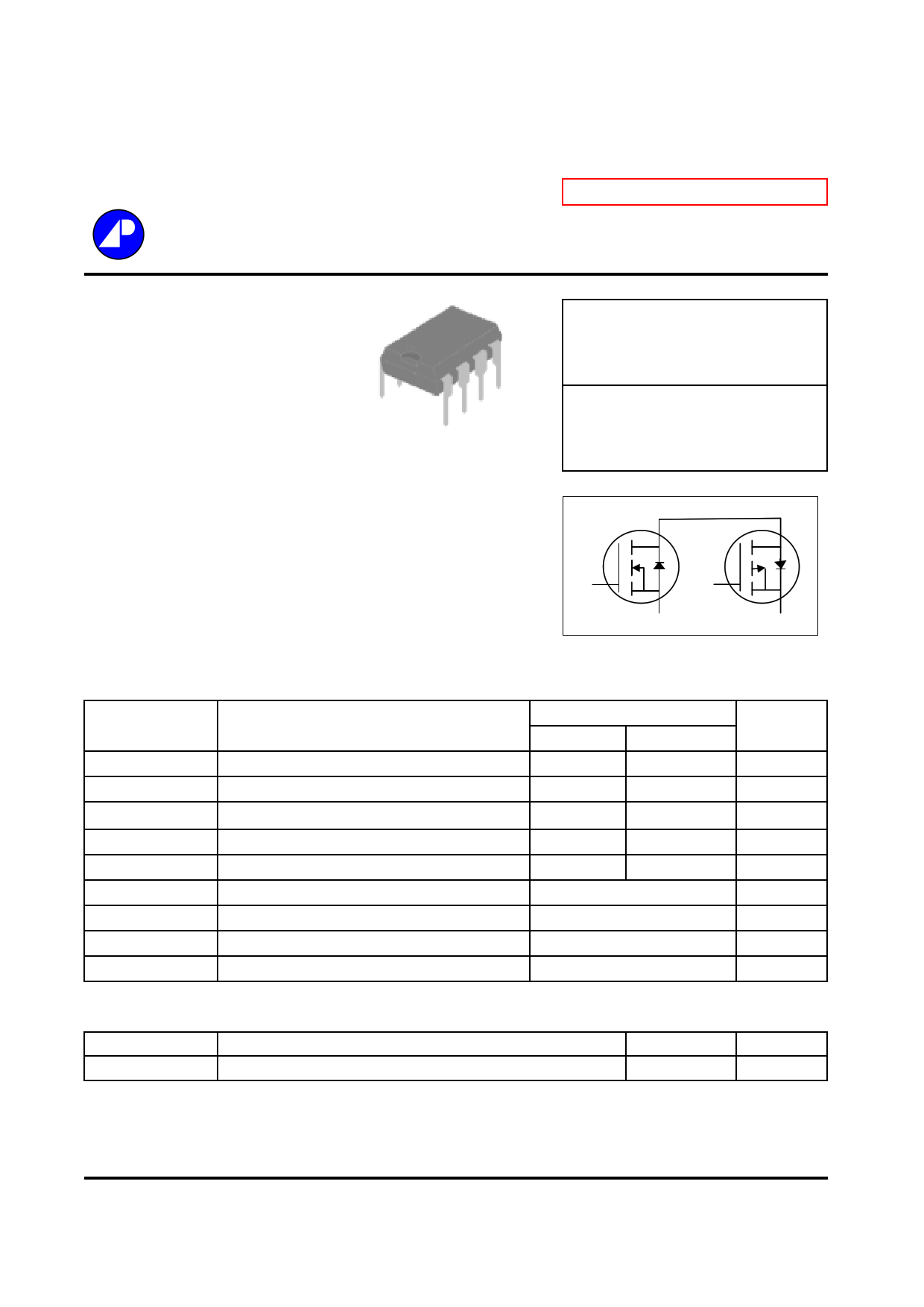
AP4501GSD
Pb Free Plating Product
N AND P-CHANNEL ENHANCEMENT
MODE POWER MOSFET
▼ Simple Drive Requirement
▼ Low On-resistance
▼ Fast Switching Characteristic
Description
D2
D2
D1
D1
PDIP-8
G2
S2
G1
S1
The Advanced Power MOSFETs from APEC provide the
designer with the best combination of fast switching,
ruggedized device design, low on-resistance and cost-
effectiveness.
N-CH
P-CH
BVDSS
RDS(ON)
ID
BVDSS
RDS(ON)
ID
D1
30V
27mΩ
7A
-30V
49mΩ
-5A
D2
G1
S1
G2
S2
Absolute Maximum Ratings
Symbol
Parameter
VDS
VGS
ID@TA=25℃
ID@TA=70℃
IDM
PD@TA=25℃
TSTG
TJ
Drain-Source Voltage
Gate-Source Voltage
Continuous Drain Current3
Continuous Drain Current3
Pulsed Drain Current1
Total Power Dissipation
Linear Derating Factor
Storage Temperature Range
Operating Junction Temperature Range
Thermal Data
Symbol
Rthj-a
Parameter
Thermal Resistance Junction-ambient3
Rating
N-channel P-channel
30 -30
±20 ±20
7 -5
5.8 -4.2
40 -30
2
0.016
-55 to 150
-55 to 150
Max.
Value
62.5
Units
V
V
A
A
A
W
W/℃
℃
℃
Unit
℃/W
Data and specifications subject to change without notice
200504042
Datasheet pdf - http://www.DataSheet4U.net/
1 page 
www.DataSheet.co.kr
N-Channel
12
I D =7.0A
9 V DS =16V
V DS =20V
V DS =24V
6
3
0
0 4 8 12
Q G , Total Gate Charge (nC)
16
Fig 7. Gate Charge Characteristics
100
100us
10
1ms
1 10ms
100ms
0.1
T A =25 o C
Single Pulse
1s
10s
DC
0.01
0.1 1 10 100
V DS , Drain-to-Source Voltage (V)
Fig 9. Maximum Safe Operating Area
VDS
90%
10%
VGS
td(on) tr
td(off)tf
Fig 11. Switching Time Waveform
AP4501GSD
f=1.0MHz
1000
C iss
C oss
C100
rss
10
1
7 13 19 25 31
V DS , Drain-to-Source Voltage (V)
Fig 8. Typical Capacitance Characteristics
1
Duty Factor = 0.5
0.2
0.1 0.1
0.05
0.01
0.02
0.01
Single Pulse
PDM
t
T
0.001
0.0001
0.001
Duty Factor = t/T
Peak Tj = PDM x Rthja + Ta
Rthja =90oC/W
0.01 0.1 1 10
t , Pulse Width (s)
100 1000
Fig 10. Effective Transient Thermal Impedance
VG
4.5V
QGS
QG
QGD
Charge
Q
Fig 12. Gate Charge Waveform
Datasheet pdf - http://www.DataSheet4U.net/
5 Page | ||
| Páginas | Total 7 Páginas | |
| PDF Descargar | [ Datasheet 4501GSD.PDF ] | |
Hoja de datos destacado
| Número de pieza | Descripción | Fabricantes |
| 4501GSD | AP4501GSD | Advanced Power Electronics |
| Número de pieza | Descripción | Fabricantes |
| SLA6805M | High Voltage 3 phase Motor Driver IC. |
Sanken |
| SDC1742 | 12- and 14-Bit Hybrid Synchro / Resolver-to-Digital Converters. |
Analog Devices |
|
DataSheet.es es una pagina web que funciona como un repositorio de manuales o hoja de datos de muchos de los productos más populares, |
| DataSheet.es | 2020 | Privacy Policy | Contacto | Buscar |