|
|
|
PDF J175 Data sheet ( Hoja de datos )
| Número de pieza | J175 | |
| Descripción | Switching | |
| Fabricantes | Micross | |
| Logotipo | ||
Hay una vista previa y un enlace de descarga de J175 (archivo pdf) en la parte inferior de esta página. Total 1 Páginas | ||
|
No Preview Available !
J175
P-CHANNEL JFET
Linear Systems replaces discontinued Siliconix J175
The J175 is a single P-Channel JFET switch
This p-channel analog switch is designed to provide low
on-resistance and fast switching. When used in
combination with the complimentary J/SST111 n-
channel family, the J175 simplifies series-shunt
switching applications
J. 175 Benefits:
FEATURES
DIRECT REPLACEMENT FOR SILICONIX J175
LOW ON RESISTANCE
LOW GATE OPERATING CURRENT
FAST SWITCHING
ABSOLUTE MAXIMUM RATINGS
@ 25°C (unless otherwise noted)
rDS(on) ≤ 125Ω
ID(off) = 10pA
t(ON) 25ns
Low Error Voltage
High-Speed Analog Circuit Performance
Negligible “Off-Error,” Excellent Accuracy
Good Frequency Response
Eliminates Additional Buffering
J175 Applications:
Maximum Temperatures
Storage Temperature
Operating Junction Temperature
Maximum Power Dissipation
Continuous Power Dissipation
MAXIMUM CURRENT
‐55°C to +150°C
‐55°C to +135°C
350mW
Analog Switches
Choppers
Sample-and-Hold
Normally “On” Switches
Current Limiters
Gate Current (Note 1)
MAXIMUM VOLTAGES
Gate to Drain Voltage
Gate to Source Voltage
IG = ‐50mA
VGDS = 30V
VGSS = 30V
J175 ELECTRICAL CHARACTERISTICS @ 25°C (unless otherwise noted)
SYMBOL
CHARACTERISTIC
MIN TYP.
MAX
UNITS
CONDITIONS
BVGSS
Gate to Source Breakdown Voltage 30
VGS(F)
VGS(off)
IDSS
IGSS
ClickIG
Gate to Source Forward Voltage
Gate to Source Cutoff Voltage
Drain to Source Saturation Current
Gate Reverse Current
Gate Operating Current
‐‐
3
‐7
‐‐
‐‐
ID(off)
Drain Cutoff Current
‐‐
‐‐ ‐‐
To‐0.7
‐‐
‐‐
0.01
0.01
‐‐
6
‐70
1
‐‐
‐0.01
‐1
IG = ‐1µA, VDS = 0V
BuyV IG = ‐1mA, VDS = 0V
VDS = ‐15V, ID = ‐10nA
VDS = ‐15V, VGS = 0V
VGS = 20V, VDS = 0V
nA VDG = ‐15V, ID = ‐1mA
VDS = ‐15V, VGS = 0V
rDS(on)
Drain to Source On Resistance
‐‐
‐‐
125
Ω
VGS = 0V, VDS = ‐0.1V
J175 SWITCHING CHARACTERISTICS @ 25°C (unless otherwise noted)
SYMBOL
CHARACTERISTIC
UNITS
CONDITIONS
td(on)
tr
td(off)
Turn On Time
Turn On Rise Time
Turn Off Time
10
15
10 ns
tf
Turn Off Fall Time
20
Note 1 ‐ Absolute maximum ratings are limiting values above which J175 serviceabil ity may be impaired.
VGS(L) = 0V
VGS(H) = 10V
See Switching Circuit
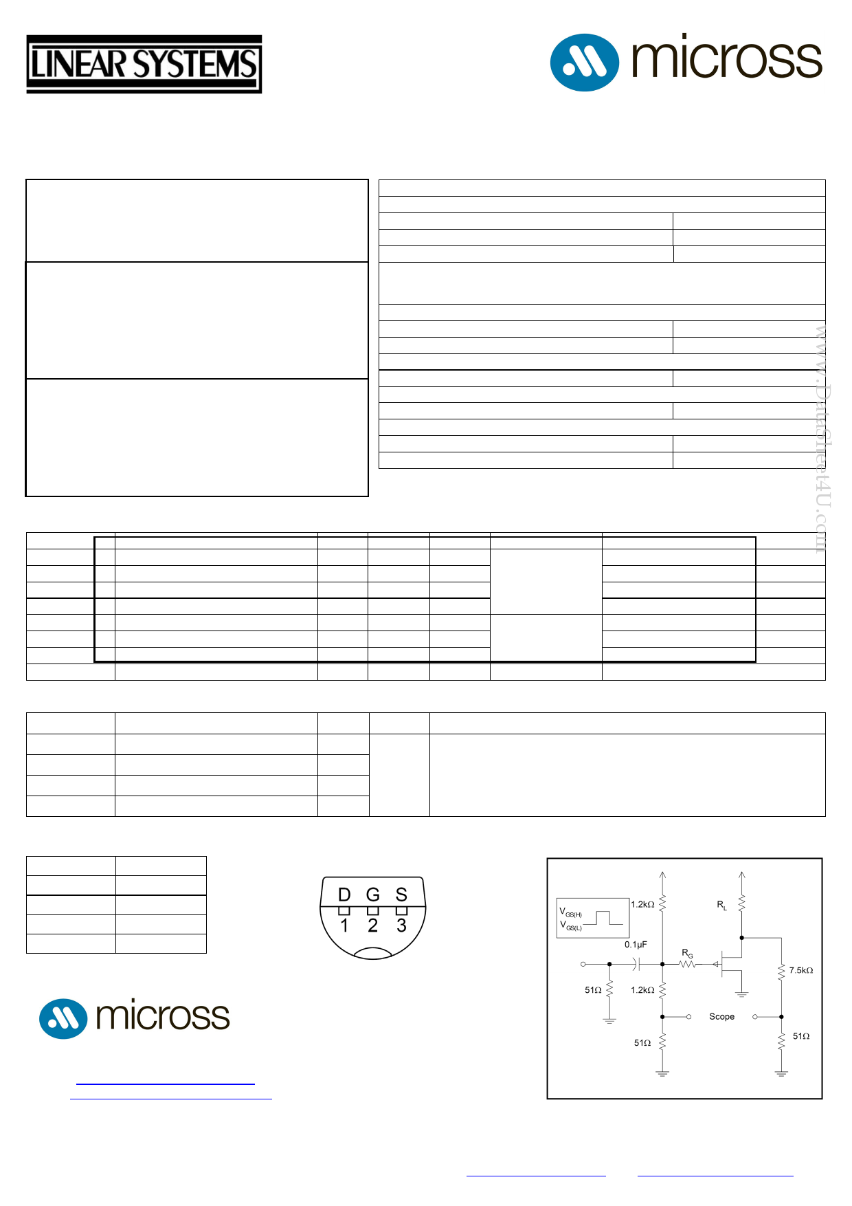
J175 SWITCHING CIRCUIT PARAMETERS T O - 9 2 ( B o t t o m V i e w ) SWITCHING CIRCUIT
VDD ‐6V
VGG 12V
RL 750Ω
RG 220Ω
ID(on)
‐7mA
Micros s Components Europe
Available Packages:
J175 in TO-92
J175 in bare die.
Tel: +44 1603 788967
Email: [email protected]
Web: http://www.micross.com/distribution
Please contact Micross for full
package and die dimensions
Information furnished by Linear Integrated Systems and Micross Components is believed to be accurate and reliable. However, no responsibility is assumed
for its use; nor for any infringement of patents or other rights of third parties which may result from its use. No license is granted by implication or otherwise
under any patent or patent rights of Linear Integrated Systems.
Micross Components Ltd, United Kingdom, Tel: +44 1603 788967, Fax: +44 1603788920, Email: [email protected] Web: www.micross.com/distribution.aspx
1 page | ||
| Páginas | Total 1 Páginas | |
| PDF Descargar | [ Datasheet J175.PDF ] | |
Hoja de datos destacado
| Número de pieza | Descripción | Fabricantes |
| J174 | P-channel silicon field-effect transistors | NXP Semiconductors |
| J174 | P-Channel Switch | Fairchild Semiconductor |
| J174 | P-Channel JFET Switch | Calogic LLC |
| J174 | SINGLE P-CHANNEL JFET SWITCH | Linear Integrated Systems |
| Número de pieza | Descripción | Fabricantes |
| SLA6805M | High Voltage 3 phase Motor Driver IC. |
Sanken |
| SDC1742 | 12- and 14-Bit Hybrid Synchro / Resolver-to-Digital Converters. |
Analog Devices |
|
DataSheet.es es una pagina web que funciona como un repositorio de manuales o hoja de datos de muchos de los productos más populares, |
| DataSheet.es | 2020 | Privacy Policy | Contacto | Buscar |