|
|
|
PDF V103A Data sheet ( Hoja de datos )
| Número de pieza | V103A | |
| Descripción | TRIPLE 10-BIT LVDS TRANSMITTER FOR VIDEO | |
| Fabricantes | Integrated Device Technology | |
| Logotipo | ||
Hay una vista previa y un enlace de descarga de V103A (archivo pdf) en la parte inferior de esta página. Total 11 Páginas | ||
|
No Preview Available !
V103A
TRIPLE 10-BIT LVDS TRANSMITTER FOR VIDEO
General Description
The V103A LVDS display interface transmitter is
primarily designed to support pixel data transmission
between a video processing engine and a digital video
display. The data rate supports up to SXGA+
resolutions and can be used in Plasma, Rear Projector,
Front Projector, CRT and LCD display applications. It
can also be used in other high-bandwidth parallel data
applications and provides a low EMI interconnect over
a low cost, low bus width cable up to several meters in
length.
The V103A converts 35 bits of CMOS/TTL data,
clocked on the rising or falling edge of an input clock
(selectable), into six LVDS (Low Voltage Differential
Signaling) serial data stream pairs. In video
applications the 35 bits is normally divided into 10 bits
for each R, G and B channel and 5 control bits.
When combined with the V104 LVDS display interface
receiver, the V103A + V104 combination provides a
35-bit wide, 90 MHz transport. The rate of each LVDS
channel is 630 Mbps for a 90MHz data input clock, 945
Mbps for 135MHz.
Features
• Pin compatible with THine THC63LVD103
• Wide pixel clock range: 8 - 135 MHz
• Guaranteed operation over -20 to +85° C ambient
temperature
• Supports a wide range of video and graphics modes
including VGA, SVGA, XGA, SXGA, SXGA+, NTSC,
PAL, SDTV, and HDTV up to 1080I or 720P
• Internal PLL requires no external loop filter
• Selectable rising or falling clock edge for data
alignment
• Compatible with Spread Spectrum clock source
• Reduced LVDS output voltage swing mode
(selectable) to minimize EMI
• CMOS/TTL data inputs can be configured for
reduced input voltage swing
• Single 3.3 V supply
• Low power consumption CMOS design
• Power down mode
• 64-pin TQFP lead free package
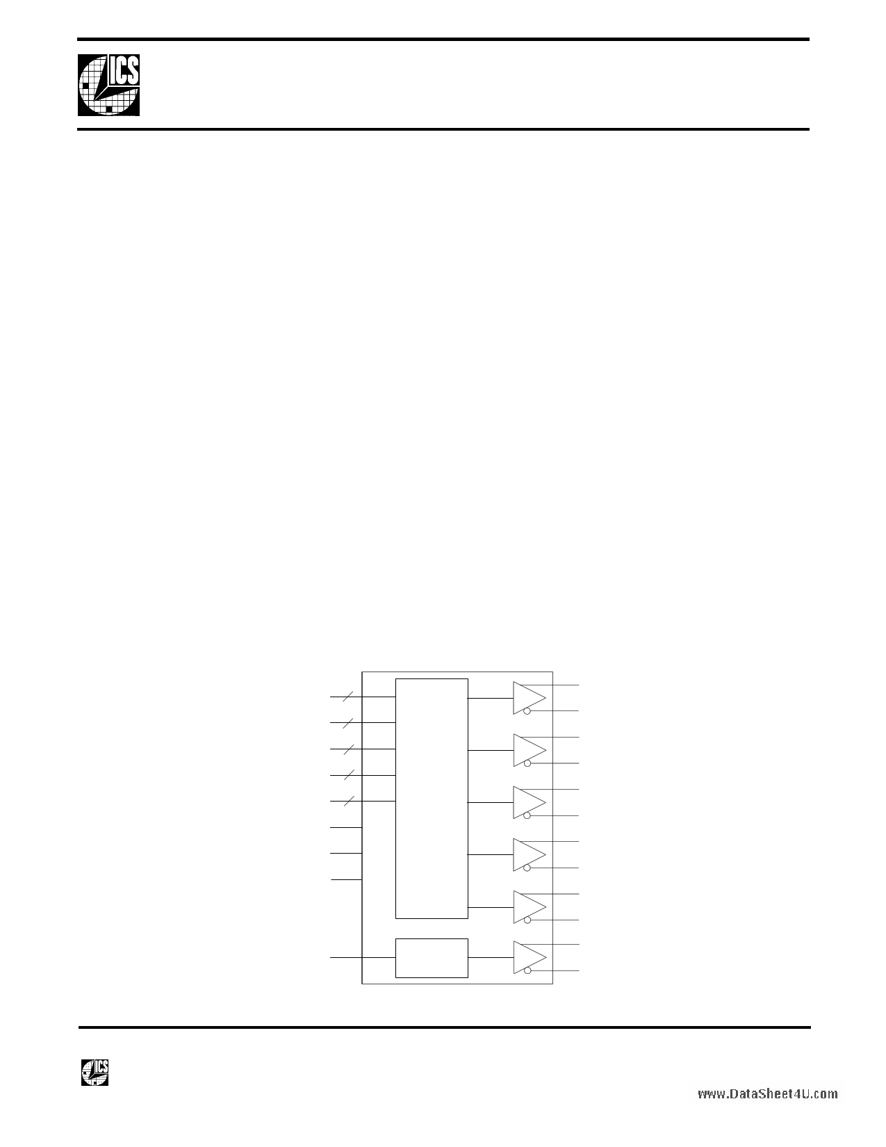
Block Diagram
TA0-6
TB0-6
TC0-6
TD0-6
TE0-6
RS
R/F
/PWDN
7
7
7
7
7
www.DataSheet4U.com
CLKIN
(8 to 135 MHz)
Parallel
to Serial
PLL
TA+
TA-
TB+
TB-
TC+
TC-
TD+
TD-
TE+
TE-
TCLK+
TCLK-
V103A Datasheet
1
11/18/05
Revision 3.2
Integrated Circuit Systems • 525 Race Street, San Jose, CA 95126 • tel (408) 297-1201 • www.icst.com
1 page 
V103A
TRIPLE 10-BIT LVDS TRANSMITTER FOR VIDEO
DC Electrical Characteristics
VDD=3.3 V ±10%, Ambient temperature -20 to +85°C
Parameter
Symbol
Conditions
Min.
Typ. Max.
CMOS/TTL Inputs, Standard Configuration
Input High Voltage
VIH RS=VCC or GND
Input Low Voltage
VIL RS=VCC or GND
Input Current
IINC 0V<VIN<VCC
CMOS/TTL Inputs, Small Input Swing Configuration
Max Input Swing Voltage
Input Reference Voltage into pin RS
High Level Input Voltage
(for small input swing condition)
VDDQ1
VREF
VSH2
VREF = VRS = VDDQ/2
VREF=VDDQ/2
Low Level Input Voltage
(for small input swing condition)
VSL2
VREF=VDDQ/2
2.00
GND
VCC
0.80
±10
1.2
VDDQ/2
+0.1V
VDDQ/2
2.8
VDDQ/2
-0.1V
Note 1: VDDQ voltage defines the max voltage of the small swing input and is not an actual input into the device.
Note 2: Small input swing voltage is applied to TA[6:0], TB[6:0], TC[6:0], TD[6:0], TE[6:0], and CLKIN.
Units
V
V
µA
V
V
V
V
LVDS Transmitter DC Specifications
Differential Output Voltage,
RL = 100Ω
Change in VOD Between Complimentary
Output States
Common Mode Voltage
Change in VOC Between Complimentary
Output States
Output Short Circuit Current
Output Tri-State Current
VOD
DVOD
Normal swing
RS = VCC
Reduced swing
RS = GND
VOC
DVOC
RL = 100Ω
IOS VOUT = 0V, RL = 100Ω
IOZ /PWDN = 0V,
VOUT = 0V to VCC
250
100
1.125
350
200
1.250
450
300
35
1.375
35
-24
±10
mV
mV
mV
V
mV
mA
µA
Supply Current
Transmitter Supply Current
Transmitter Supply Current
www.DataSheet4U.com
Transmitter Power Down Supply Current
ITCCG
ITCCW
ITCCS
RL = 100Ω, CL=5 pF,
f = 85 MHz
VCC = 3.3 V, RS = VCC f =135 MHz
Gray Scale Pattern
RL = 100Ω, CL=5 pF,
f = 85 MHz
VCC = 3.3 V, RS = GND f =135 MHz
Gray Scale Pattern
RL = 100Ω, CL = 5 pF,
f = 85 MHz
VCC = 3.3 V, RS = VCC f =135 MHz
Worst Case Pattern
RL = 100Ω, CL= 5 pF,
f = 85 MHz
VCC = 3.3 V, RS = GND f =135 MHz
Worst Case Pattern
/PWDN = L
58
70
44
56
69
87
55
73
64 mA
76 mA
50 mA
62 mA
75 mA
93 mA
61 mA
79 mA
10 µA
V103A Datasheet
5
11/18/05
Revision 3.2
Integrated Circuit Systems • 525 Race Street, San Jose, CA 95126 • tel (408) 297-1201 • www.icst.com
5 Page 
V103A
TRIPLE 10-BIT LVDS TRANSMITTER FOR VIDEO
Package Outline and Package Dimensions (64-pin TQFP)
Package dimensions are kept current with JEDEC Publication No. 95, variation ACD.
ALL DIMENSIONS ARE IN MILLIMETERS.
SYMBOL
N
A
A1
A2
b
c
D
D1
D2
E
E1
E2
e
L
θ
ccc
D3&E3
MIN/MAX
64
-- / 1.20
0.05 / 0.15
0.95 / 1.05
0.17 / 0.27
0.09 / 0.20
12.00 BASIC
10.00 BASIC
7.50 Ref.
12.00 BASIC
10.00 BASIC
7.50 Ref.
0.50 BASIC
0.45 / 0.75
0° / 7°
-- / 0.08
-
Ordering Information
Part / Order Number
V103AYLF
V103AYLFT
Marking
V103AYLF
V103AYLF
Shipping Packaging
Tray (160 units per tray)
Tape and Reel
Package
64-pin TQFP
64-pin TQFP
Temperature
-20 to +85° C
-20 to +85° C
The “LF” part number suffix denotes the device as Lead (Pb) Free and that the device is RoHS compliant.
While the information presented herein has been checked for both accuracy and reliability, Integrated Circuit Systems (ICS) assumes no
responsibility for either its use or for the infringement of any patents or other rights of third parties, which would result from its use. No other
www.DcaitracuSihtse,epta4tUen.ctso,mor licenses are implied. This product is intended for use in normal commercial applications. Any other applications such as
those requiring extended temperature range, high reliability, or other extraordinary environmental requirements are not recommended without
additional processing by ICS. ICS reserves the right to change any circuitry or specifications without notice. ICS does not authorize or warrant
any ICS product for use in life support devices or critical medical instruments.
V103A Datasheet
11
11/18/05
Revision 3.2
Integrated Circuit Systems • 525 Race Street, San Jose, CA 95126 • tel (408) 297-1201 • www.icst.com
11 Page | ||
| Páginas | Total 11 Páginas | |
| PDF Descargar | [ Datasheet V103A.PDF ] | |
Hoja de datos destacado
| Número de pieza | Descripción | Fabricantes |
| V103 | TRIPLE 10-BIT LVDS TRANSMITTER FOR VIDEO | Integrated Device Technology |
| V103A | TRIPLE 10-BIT LVDS TRANSMITTER FOR VIDEO | Integrated Device Technology |
| Número de pieza | Descripción | Fabricantes |
| SLA6805M | High Voltage 3 phase Motor Driver IC. |
Sanken |
| SDC1742 | 12- and 14-Bit Hybrid Synchro / Resolver-to-Digital Converters. |
Analog Devices |
|
DataSheet.es es una pagina web que funciona como un repositorio de manuales o hoja de datos de muchos de los productos más populares, |
| DataSheet.es | 2020 | Privacy Policy | Contacto | Buscar |