|
|
|
PDF CY14B512P Data sheet ( Hoja de datos )
| Número de pieza | CY14B512P | |
| Descripción | 512-Kbit (64 K X 8) Serial (SPI) nvSRAM | |
| Fabricantes | Cypress Semiconductor | |
| Logotipo | ||
Hay una vista previa y un enlace de descarga de CY14B512P (archivo pdf) en la parte inferior de esta página. Total 30 Páginas | ||
|
No Preview Available !
CY14B512P
512-Kbit (64 K × 8) Serial (SPI) nvSRAM
with Real Time Clock
512-Kbit (64 K × 8) Serial (SPI) nvSRAM with Real Time Clock
Features
■ 512-Kbit nonvolatile static random access memory (nvSRAM)
❐ Internally organized as 64 K × 8
❐ STORE to QuantumTrap nonvolatile elements initiated
automatically on power-down (AutoStore) or by the user
using HSB pin (Hardware STORE) or SPI instruction
(Software STORE)
❐ RECALL to SRAM initiated on power-up (Power-Up
RECALL) or by serial peripheral interface (SPI) instruction
(Software RECALL)
❐ Automatic STORE on power-down with a small capacitor
■ High reliability
❐ Infinite read, write, and RECALL cycles
❐ 1 million STORE cycles to QuantumTrap
❐ Data retention: 20 years
■ Real time clock (RTC)
❐ Full featured RTC
❐ Watchdog timer
❐ Clock alarm with programmable interrupts
❐ Capacitor or battery backup for RTC
❐ Backup current of 0.35 µA (typical)
■ High-speed SPI
❐ 40 MHz clock rate – SRAM memory access
❐ 25 MHz clock rate – RTC memory access
❐ Supports SPI mode 0 (0,0) and mode 3 (1,1)
■ Write protection
❐ Hardware protection using Write Protect (WP) pin
❐ Software protection using Write Disable instruction
❐ Software block protection for 1/4, 1/2, or entire array
■ Low power consumption
❐ Single 3 V + 20%, –10% operation
❐ Average active current of 10 mA at 40 MHz operation
■ Industry standard configurations
❐ Industrial temperature
❐ 16-pin small outline integrated circuit (SOIC) package
❐ Restriction of hazardous substances (RoHS) compliant
Overview
The Cypress CY14B512P combines a 512-Kbit nvSRAM[1] with
a full-featured real time clock in a monolithic integrated circuit
with serial SPI interface. The memory is organized as 64 K words
of 8 bits each. The embedded nonvolatile elements incorporate
the QuantumTrap technology, creating the world’s most reliable
nonvolatile memory. The SRAM provides infinite read and write
cycles, while the QuantumTrap cells provide highly reliable
nonvolatile storage of data. Data transfers from SRAM to the
nonvolatile elements (STORE operation) takes place
automatically at power-down. On power-up, data is restored to
the SRAM from the nonvolatile memory (RECALL operation).
The STORE and RECALL operations can also be initiated by the
user through SPI instruction.
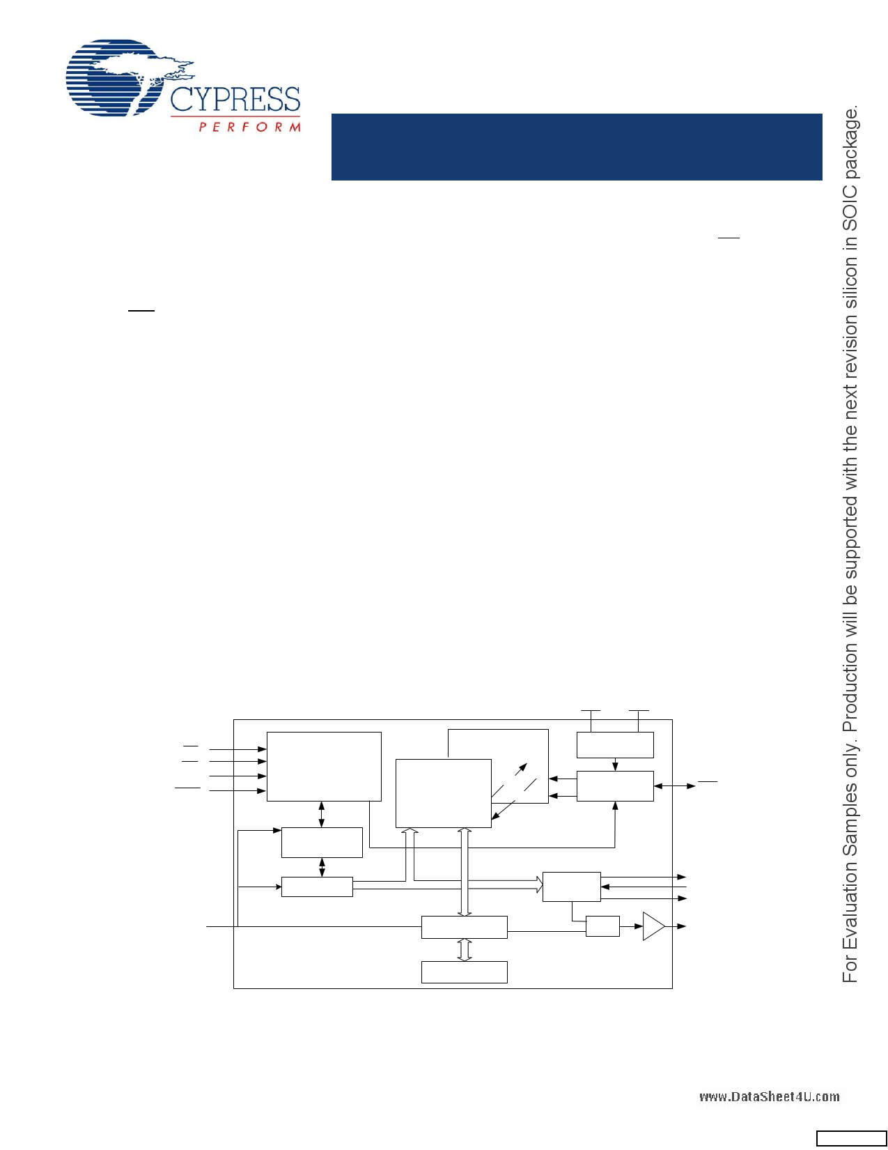
Logic Block Diagram
VCC
VCAP
CS
WP
SCK
HOLD
Instruction decode
Write protect
Control logic
QuantumTrap
64 K X 8
SRAM Array
64 K X 8
STORE
RECALL
Power Control
STORE/RECALL
Control
HSB
SI
www.DataSheet4U.com
Instruction
register
Address
Decoder
A0-A15
D0-D7
Data I/O register
Status Register
RTC
MUX
Xout
X in
INT
SO
Note
1. This device is referred to as nvSRAM throughout the document.
Cypress Semiconductor Corporation • 198 Champion Court
Document #: 001-53872 Rev. *E
• San Jose, CA 95134-1709 • 408-943-2600
Revised January 12, 2011
[+] Feedback
1 page 
CY14B512P
Figure 2 shows the proper connection of the storage capacitor
(VCAP) for AutoStore operation. Refer to DC Electrical
Characteristics on page 25 for the size of the VCAP.
Figure 2. AutoStore Mode
VCC
0.1 uF
VCC
CS VCAP
VSS
VCAP
Software STORE Operation
Software STORE allows the user to trigger a STORE operation
through a special SPI instruction. The STORE operation is
initiated by executing a STORE instruction regardless of whether
a write has been performed since the last NV operation.
A STORE cycle takes tSTORE time to complete, during which all
the memory accesses to nvSRAM are inhibited. The RDY bit of
the Status Register or the HSB pin may be polled to find the
Ready / Busy status of the nvSRAM. After the tSTORE cycle time
is completed, the SRAM is activated again for read and write
operations.
Hardware STORE and HSB Pin Operation
The HSB pin in CY14B512P is used to control and acknowledge
STORE operations. If no STORE/RECALL is in progress, this pin
can be used to request a Hardware STORE cycle. When the
HSB pin is driven LOW, the CY14B512P conditionally initiates a
STORE operation after tDELAY duration. A STORE cycle starts
only if a write to the SRAM was performed since the last STORE
or RECALL cycle. Reads and writes to the memory are inhibited
for tSTORE duration or as long as HSB pin is LOW.
The HSB pin also acts as an open drain driver (internal 100-kΩ
weak pull-up resistor) that is internally driven LOW to indicate a
busy condition when the STORE (initiated by any means) is in
progress.
Note After each Hardware and Software STORE operation HSB
wwwi.sDdartiavSehneHetI4GUH.cfomr a short time (tHHHD) with standard output high
current and then remains HIGH by an internal 100-kΩ pull-up
resistor.
Note For successfull last data byte STORE, a hardware store
should be initiated atleast one clock cycle after the last data bit
D0 is recieved.
Upon completion of the STORE operation, the nvSRAM memory
access is inhibited for tLZHSB time after HSB pin returns HIGH.
The HSB pin must be left unconnected if not used.
RECALL Operation
A RECALL operation transfers the data stored in the nonvolatile
QuantumTrap elements to the SRAM. In CY14B512P, a
RECALL may be initiated in two ways: Hardware RECALL,
initiated on power-up; and Software RECALL, initiated by a SPI
RECALL instruction.
Internally, RECALL is a two step procedure. First, the SRAM data
is cleared. Next, the nonvolatile information is transferred into the
SRAM cells. All memory accesses are inhibited while a RECALL
cycle is in progress. The RECALL operation does not alter the
data in the nonvolatile elements.
Hardware RECALL (Power-Up)
During power-up, when VCC crosses VSWITCH, an automatic
RECALL sequence is initiated, which transfers the content of
nonvolatile memory on to the SRAM.
A Power-Up RECALL cycle takes tFA time to complete and the
memory access is disabled during this time. HSB pin is used to
detect the Ready status of the device.
Software RECALL
Software RECALL allows the user to initiate a RECALL operation
to restore the content of nonvolatile memory on to the SRAM. In
CY14B512P, this can be done by issuing a RECALL instruction
in SPI.
A Software RECALL takes tRECALL time to complete during
which all memory accesses to nvSRAM are inhibited. The
controller must provide sufficient delay for the RECALL operation
to complete before issuing any memory access instructions.
Disabling and Enabling AutoStore
If the application does not require the AutoStore feature, it can
be disabled in CY14B512P by using the ASDISB instruction. If
this is done, the nvSRAM does not perform a STORE operation
at power-down.
AutoStore can be re-enabled by using the ASENB instruction.
However, these operations are not nonvolatile and if the user
needs this setting to survive the power cycle, a STORE operation
must be performed following AutoStore Disable or Enable
operation.
Note CY14B512P comes from the factory with AutoStore
Enabled.
Note If AutoStore is disabled and VCAP is not required, then the
VCAP pin must be left open. The VCAP pin must never be
connected to ground. The Power-Up RECALL operation cannot
be disabled in any case.
Document #: 001-53872 Rev. *E
Page 5 of 36
[+] Feedback
5 Page 
CY14B512P
Hardware Write Protection (WP Pin)
The write protect pin (WP) is used to provide hardware write
protection. WP pin allows all normal read and write operations
when held HIGH. When the WP pin is brought LOW and WPEN
bit is ‘1’ all write operations to the Status Register are inhibited.
The hardware write protection function is blocked when the
WPEN bit is ‘0’. This allows the user to install the CY14B512P in
a system with the WP pin tied to ground, and still write to the
Status Register.
WP pin can be used along with WPEN and block protect bits
(BP1 and BP0) of the Status Register to inhibit writes to memory.
When WP pin is LOW and WPEN is set to ‘1’, any modifications
to the Status Register are disabled. Therefore, the memory is
protected by setting the BP0 and BP1 bits and the WP pin inhibits
any modification of the Status Register bits, providing hardware
write protection.
Note WP going LOW when CS is still LOW has no effect on any
of the ongoing write operations to the Status Register.
Table 6 summarizes all the protection features provided in the
CY14B512P.
Table 6. Write Protection Operation
WPEN WP
XX
0X
1 LOW
1 HIGH
WEN
Protected Unprotected
Blocks
Blocks
Status
Register
0 Protected Protected Protected
1 Protected Writable Writable
1 Protected Writable Protected
1 Protected Writable Writable
Memory Access
All memory accesses are done using the READ and WRITE
instructions. These instructions cannot be used while a STORE
or RECALL cycle is in progress. A STORE cycle in progress is
indicated by the RDY bit of the Status Register and the HSB pin.
Read Sequence (READ) instruction
The read operations on CY14B512P are performed by giving the
instruction on the SI pin and reading the output on SO pin. The
following sequence needs to be followed for a read operation:
After the CS line is pulled LOW to select a device, the read
opcode is transmitted through the SI line followed by two bytes
of address. After the last address bit is transmitted on the SI pin,
the data (D7-D0) at the specific address is shifted out on the SO
line on the falling edge of SCK starting with D7. Any other data
on SI line after the last address bit is ignored.
CY14B512P allows reads to be performed in bursts through SPI
which can be used to read consecutive addresses without
issuing a new READ instruction. If only one byte is to be read,
the CS line must be driven HIGH after one byte of data comes
out. However, the read sequence may be continued by holding
the CS line LOW and the address is automatically incremented
and data continues to shift out on SO pin. When the last data
memory address (0xFFFF) is reached, the address rolls over to
0x0000 and the device continues to read.
Write Sequence (WRITE) instruction
The write operations on CY14B512P are performed through the
SI pin. To perform a write operation CY14B512P, if the device is
write disabled, then the device must first be Write Enabled
through the WREN instruction. When the writes are enabled
(WEN = ‘1’), WRITE instruction is issued after the falling edge of
CS. A WRITE instruction constitutes transmitting the WRITE
opcode on SI line followed by 2 bytes of address and the data
(D7-D0) which is to be written.
CY14B512P allows writes to be performed in bursts through SPI
which can be used to write consecutive addresses without
issuing a new WRITE instruction. If only one byte is to be written,
the CS line must be driven HIGH after the D0 (LSB of data) is
transmitted. However, if more bytes are to be written, CS line
must be held LOW and address incremented automatically. The
following bytes on the SI line are treated as data bytes and
written in the successive addresses. When the last data memory
address (0xFFFF) is reached, the address rolls over to 0x0000
and the device continues to write. The WEN bit is reset to ‘0’ on
completion of a WRITE sequence.
Note When a burst write reaches a protected block address, it
continues the address increment into the protected space but
does not write any data to the protected memory. If the address
roll over takes the burst write to unprotected space, it resumes
writes. The same operation is true if a burst write is initiated
within a write protected block.
Figure 10. Read Instruction Timing
CS
SCK
0 1 2 34 5 67 0 1 23 45 6 7
12 13 14 15 0 1 2 3 4 5 6 7
Op-Code
16-bit Address
www.DataSShI eet4U.co0m 0 0 0 0 0 1 1 15 14 13 12 11 10 9 8
MSB
HI-Z
SO
32
10
LSB
D7 D6 D5 D4 D3 D2 D1 D0
MSB
Data
LSB
Document #: 001-53872 Rev. *E
Page 11 of 36
[+] Feedback
11 Page | ||
| Páginas | Total 30 Páginas | |
| PDF Descargar | [ Datasheet CY14B512P.PDF ] | |
Hoja de datos destacado
| Número de pieza | Descripción | Fabricantes |
| CY14B512I | 512-Kbit (64 K x 8) Serial (I2C) nvSRAM | Cypress Semiconductor |
| CY14B512J | 512-Kbit (64 K x 8) Serial (I2C) nvSRAM | Cypress Semiconductor |
| CY14B512P | 512-Kbit (64 K X 8) Serial (SPI) nvSRAM | Cypress Semiconductor |
| CY14B512PA | 512-Kbit (64 K x 8) SPI nvSRAM | Cypress Semiconductor |
| Número de pieza | Descripción | Fabricantes |
| SLA6805M | High Voltage 3 phase Motor Driver IC. |
Sanken |
| SDC1742 | 12- and 14-Bit Hybrid Synchro / Resolver-to-Digital Converters. |
Analog Devices |
|
DataSheet.es es una pagina web que funciona como un repositorio de manuales o hoja de datos de muchos de los productos más populares, |
| DataSheet.es | 2020 | Privacy Policy | Contacto | Buscar |