|
|
|
PDF 7915CV Data sheet ( Hoja de datos )
| Número de pieza | 7915CV | |
| Descripción | Negative voltage regulators | |
| Fabricantes | STMicroelectronics | |
| Logotipo | ||
Hay una vista previa y un enlace de descarga de 7915CV (archivo pdf) en la parte inferior de esta página. Total 24 Páginas | ||
|
No Preview Available !
L7900 series
Negative voltage regulators
Feature summary
■ Output current up to 1.5A
■ Output voltages of -5; -6; -8; -12; -15; -18; -20;
-24V
■ Thermal overload protection
■ Short circuit protection
■ Output transition SOA protection
Description
The L7900 series of three-terminal negative
regulators is available in TO-220, TO-220FP, TO-3
and D2PAK packages and several fixed output
voltages, making it useful in a wide range of
applications. These regulators can provide local
on-card regulation, eliminating the distribution
problems associated with single point regulation;
furthermore, having the same voltage option as
the L7800 positive standard series, they are
particularly suited for split power supplies. If
adequate heat sinking is provided, they can
deliver over 1.5A output current.
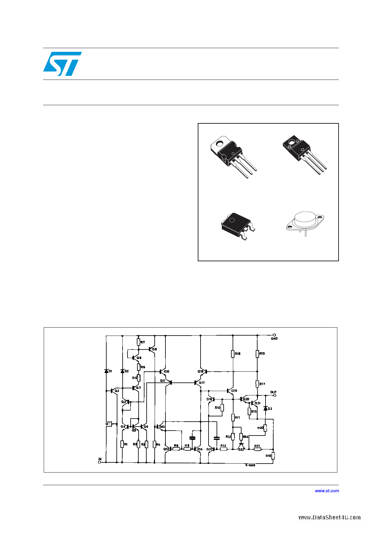
Schematic diagram
TO-220
TO-220FP
D2PAK
TO-3
Although designed primarily as fixed voltage
regulators, these devices can be used with
external components to obtain adjustable
voltages and currents.
www.DataSheet4U.com
January 2007
Rev. 11
1/24
www.st.com
24
1 page 
L7900 series
3 Test circuit
Figure 2. Test circuit
Test circuit
www.DataSheet4U.com
5/24
5 Page 
L7900 series
5 Application information
Figure 3. Fixed output regulator
Application information
1. To specify an output voltage, substitute voltage value for "XX".
2. Required for stability. For value given, capacitor must be solid tantalum. If aluminium electrolytics are used,
at least ten times value should be selected. C1 is required if regulator is located an appreciable distance
from power supply filter.
3. To improve transient response. If large capacitors are used, a high current diode from input to output
(1N4001 or similar) should be introduced to protect the device from momentary input short circuit.
Figure 4. Split power supply (± 15V - 1 A)
(*) Against potential latch-up problems.
www.DataSheet4U.com
11/24
11 Page | ||
| Páginas | Total 24 Páginas | |
| PDF Descargar | [ Datasheet 7915CV.PDF ] | |
Hoja de datos destacado
| Número de pieza | Descripción | Fabricantes |
| 7915CV | Negative voltage regulators | STMicroelectronics |
| Número de pieza | Descripción | Fabricantes |
| SLA6805M | High Voltage 3 phase Motor Driver IC. |
Sanken |
| SDC1742 | 12- and 14-Bit Hybrid Synchro / Resolver-to-Digital Converters. |
Analog Devices |
|
DataSheet.es es una pagina web que funciona como un repositorio de manuales o hoja de datos de muchos de los productos más populares, |
| DataSheet.es | 2020 | Privacy Policy | Contacto | Buscar |