|
|
|
PDF N04M163WL1A Data sheet ( Hoja de datos )
| Número de pieza | N04M163WL1A | |
| Descripción | 4Mb Ultra-Low Power Asynchronous Medical CMOS SRAM 256Kx16 bit | |
| Fabricantes | NanoAmp Solutions | |
| Logotipo | ||
Hay una vista previa y un enlace de descarga de N04M163WL1A (archivo pdf) en la parte inferior de esta página. Total 9 Páginas | ||
|
No Preview Available !
NanoAmp Solutions, Inc.
N04M163WL1A670 North McCarthy Blvd. Suite 220, Milpitas, CA 95035
ph: 408-935-7777, FAX: 408-935-7770
www.nanoamp.com
www.DataSheet4U.com
4Mb Ultra-Low Power Asynchronous Medical CMOS SRAM
256Kx16 bit
Overview
Features
The N04M163WL1A is an integrated memory
device intended for non life-support (Class 1 or
2) medical applications. This device is a 4
megabit memory organized as 262,144 words by
16 bits. The device is designed and fabricated
using NanoAmp’s advanced CMOS technology
with reliability inhancements for medical users. The
base design is the same as NanoAmp’s
N04M1618L2A, which has further reliability
processing for life-support (Class 3) medical
applications. The device operates with two chip
enable (CE1 and CE2) controls and output enable
(OE) to allow for easy memory expansion. Byte
controls (UB and LB) allow the upper and lower
bytes to be accessed independently and can also
be used to deselect the device. This device is
optimal for various applications where low-power is
critical such as battery backup and hand-held
devices. The device can operate over a very wide
temperature range of -40oC to +85oC and is
available in a JEDEC standard BGA package
Product Family
• Single Wide Power Supply Range
2.3 to 3.6 Volts
• Very low standby current
4.0µA at 3.0V (Typical)
• Very low operating current
2.0mA at 3.0V and 1µs (Typical)
• Very low Page Mode operating current
0.8mA at 3.0V and 1µs (Typical)
• Simple memory control
Dual Chip Enables (CE1 and CE2)
Byte control for independent byte operation
Output Enable (OE) for memory expansion
• Low voltage data retention
Vcc = 1.8V
• Special processing for Soft Error Rate (SER)
reduction
• Automatic power down to standby mode
• Compact space saving BGA package avail-
able
Part Number Package Type
Operating
Power
Temperature Supply (Vcc)
Speed
Standby
Operating
Current (ISB), Current (Icc),
Max Max
N04M163WL1AB 48 - BGA
N04M163WL1AT 44 - TSOP II
N04M163WL1AD Known Good Die
-40oC to +85oC
2.3V - 3.6V
70ns @ 2.7V
100ns @ 2.3V
20 µA
3 mA @ 1MHz
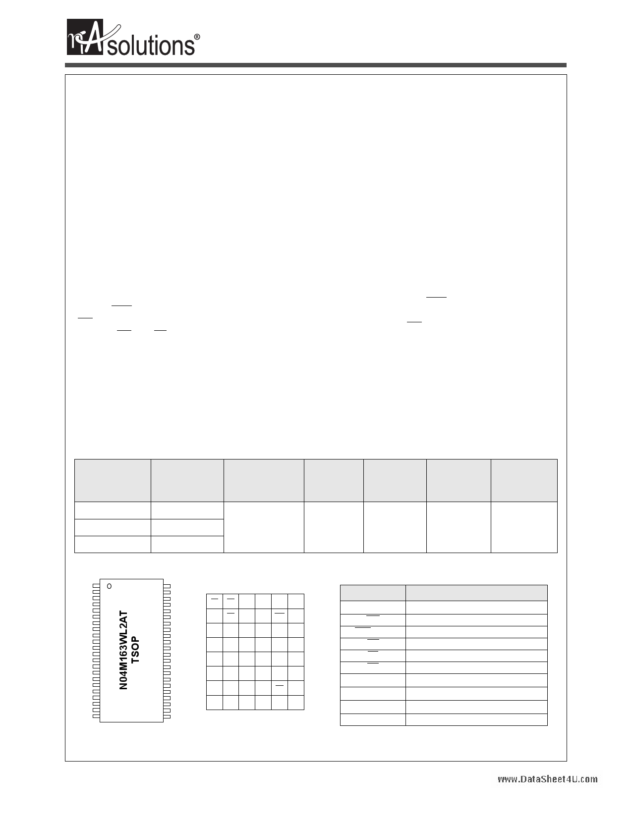
Pin Configurations
A4
A3
A2
A1
A0
CE1#
I/O0
I/O1
I/O2
I/O3
VCC
VSS
I/O15
I/O14
I/O13
I/O12
WE#
A16
A15
A14
A13
A12
1 PIN
2 ONE
3
4
5
6
7
8
9
10
11
12
13
14
15
16
17
18
19
20
21
22
44 A5
43 A6
123456
A42 A7
41 OE#
LB OE A0 A1 A2 CE2
40 UB#
B39 LB#
I/O8 UB A3 A4 CE1 I/O0
38 I/O4
C37 I/O5
36 I/O6
I/O9 I/O10 A5 A6 I/O1 I/O2
D35 I/O7
34 VSS
VSS I/O11 A17 A7 I/O3 VCC
E33 VCC
32 I/O11
VCC I/O12 NC A16 I/O4 VSS
31 I/O10
F30 I/O9
29 I/O8
I/O14 I/O13 A14 A15 I/O5 I/O6
G28 CE2
27 A8
I/O15 NC A12 A13 WE I/O7
26 A9
25 A10
H NC A8 A9 A10 A11 NC
24 A11
23 A17
48 Pin BGA (top)
6 x 8 mm
Pin Descriptions
Pin Name
A0-A17
WE
CE1, CE2
OE
LB
UB
I/O0-I/O15
VCC
VSS
NC
Pin Function
Address Inputs
Write Enable Input
Chip Enable Input
Output Enable Input
Lower Byte Enable Input
Upper Byte Enable Input
Data Inputs/Outputs
Power
Ground
Not Connected
Stock No. 23210-01 11/01/02
The specifications of this device are subject to change without notice. For latest documentation see http://www.nanoamp.com.
1
1 page 
NanoAmp Solutions, Inc.
Timing Test Conditions
Item
Input Pulse Level
Input Rise and Fall Time
Input and Output Timing Reference Levels
Output Load
Operating Temperature
Timing
Item
Read Cycle Time
Address Access Time
Chip Enable to Valid Output
Output Enable to Valid Output
Chip Enable to Low-Z output
Output Enable to Low-Z Output
Chip Disable to High-Z Output
Output Disable to High-Z Output
Output Hold from Address Change
Write Cycle Time
Chip Enable to End of Write
Address Valid to End of Write
Write Pulse Width
Address Setup Time
Write Recovery Time
Write to High-Z Output
Data to Write Time Overlap
Data Hold from Write Time
End Write to Low-Z Output
Symbol
tRC
tAA
tCO
tOE
tLZ
tOLZ
tHZ
tOHZ
tOH
tWC
tCW
tAW
tWP
tAS
tWR
tWHZ
tDW
tDH
tOW
N04M163WL1Awww.DataSheet4U.com
0.1VCC to 0.9 VCC
5ns
0.5 VCC
CL = 30pF
-40 to +85 oC
2.3 - 3.6 V
Min.
Max.
100
100
100
35
15
10
0 30
0 30
15
100
70
70
50
0
0
30
50
0
10
2.7 - 3.6 V
Min.
Max.
70
70
70
35
10
5
0 20
0 20
10
70
50
50
40
0
0
20
40
0
5
Units
ns
ns
ns
ns
ns
ns
ns
ns
ns
ns
ns
ns
ns
ns
ns
ns
ns
ns
ns
Stock No. 23210-01 11/01/02
The specifications of this device are subject to change without notice. For latest documentation see http://www.nanoamp.com.
5
5 Page | ||
| Páginas | Total 9 Páginas | |
| PDF Descargar | [ Datasheet N04M163WL1A.PDF ] | |
Hoja de datos destacado
| Número de pieza | Descripción | Fabricantes |
| N04M163WL1A | 4Mb Ultra-Low Power Asynchronous Medical CMOS SRAM 256Kx16 bit | NanoAmp Solutions |
| Número de pieza | Descripción | Fabricantes |
| SLA6805M | High Voltage 3 phase Motor Driver IC. |
Sanken |
| SDC1742 | 12- and 14-Bit Hybrid Synchro / Resolver-to-Digital Converters. |
Analog Devices |
|
DataSheet.es es una pagina web que funciona como un repositorio de manuales o hoja de datos de muchos de los productos más populares, |
| DataSheet.es | 2020 | Privacy Policy | Contacto | Buscar |