|
|
|
PDF AD7147A Data sheet ( Hoja de datos )
| Número de pieza | AD7147A | |
| Descripción | CapTouch Programmable Controller | |
| Fabricantes | Analog Devices | |
| Logotipo | ||
Hay una vista previa y un enlace de descarga de AD7147A (archivo pdf) en la parte inferior de esta página. Total 30 Páginas | ||
|
No Preview Available !
www.DataSheet4U.com
CapTouch Programmable Controller for
Single-Electrode Capacitance Sensors
AD7147A
FEATURES
Programmable capacitance-to-digital converter (CDC)
Femtofarad (ff) resolution
13 capacitance sensor inputs
9 ms update rate, all 13 sensor inputs
No external RC components required
Automatic conversion sequencer
On-chip automatic calibration logic
Automatic compensation for environmental changes
Automatic adaptive threshold and sensitivity levels
Register map is compatible with the AD714x
On-chip RAM to store calibration data
Serial peripheral interface (SPI) (AD7147A)
I2C-compatible serial interface (AD7147A-1)
Separate VDRIVE level for serial interface
Interrupt output and general-purpose input/output (GPIO)
25-ball, 2.3 mm × 2.1 mm WLCSP
2.6 V to 3.6 V supply voltage
Low operating current
Full power mode: 1 mA
Low power mode: 28.96 μA
APPLICATIONS
Cell phones
Personal music and multimedia players
Smart handheld devices
Television, A/V, and remote controls
Gaming consoles
Digital still cameras
GENERAL DESCRIPTION
The AD7147A CapTouch™ controller is designed for use with
capacitance sensors implementing functions such as buttons,
scroll bars, and wheels. The sensors need only one PCB layer,
enabling ultrathin applications.
The AD7147A is an integrated CDC with on-chip environmen-
tal calibration. The CDC has 13 inputs channeled through a
switch matrix to a 16-bit, 250 kHz sigma-delta (Σ-Δ) converter.
The CDC is capable of sensing changes in the capacitance of the
external sensors and uses this information to register a sensor
activation. By programming the registers, the user has full control
over the CDC setup.
High resolution sensors require minor software to run on the
host processor and may require two PCB layers.
CIN0 D3
CIN1 A3
CIN2 B3
CIN3 A4
CIN4 C3
CIN5 A5
CIN6 B4
CIN7 B5
CIN8 C4
CIN9 C5
CIN10 D4
CIN11 D5
CIN12 E5
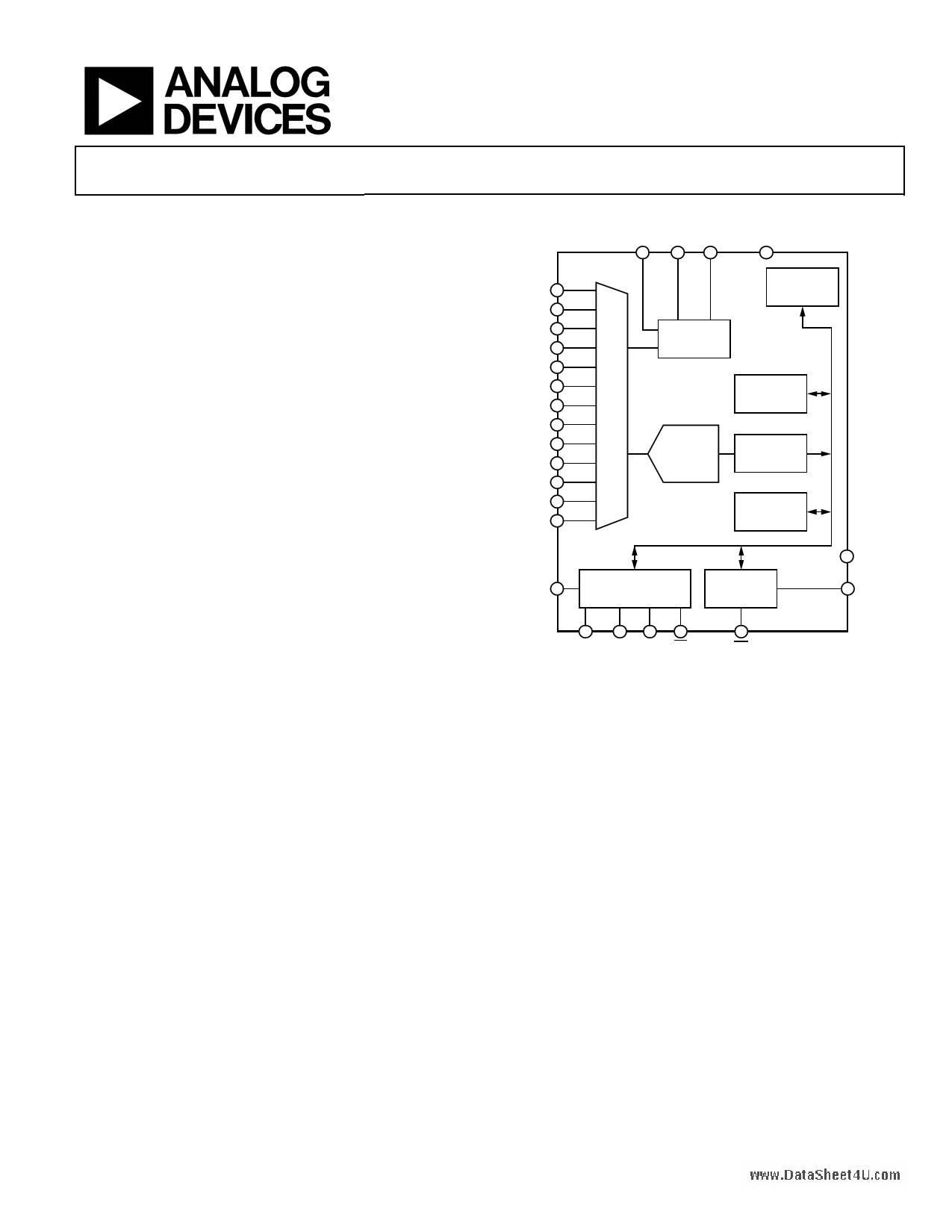
FUNCTIONAL BLOCK DIAGRAM
ACSHIELD VCC GND
E4 D2 E2
BIAS
E3
POWER-ON
RESET LOGIC
EXCITATION
SOURCE
AD7147A
CALIBRATION
RAM
16-BIT
Σ-Δ
CDC
CALIBRATION
ENGINE
CONTROL
AND DATA
REGISTERS
VDRIVE C2
SERIAL INTERFACE
AND CONTROL LOGIC
INTERRUPT
AND GPIO
LOGIC
B2 NC
A2 GPIO
E1 D1 C1 B1
A1
SDO SDI SCLK CS
(SDA) (ADD0)
(ADD1)
INT
NOTES
1. PIN NAMES IN PARENTHESES ARE FOR THE AD7147A-1.
Figure 1.
The AD7147A is designed for single electrode capacitance
sensors (grounded sensors). There is an active shield output to
minimize noise pickup in the sensor.
The AD7147A has on-chip calibration logic to compensate for
changes in the ambient environment. The calibration sequence
is performed automatically and at continuous intervals as long
as the sensors are not touched. This ensures that there are no
false or nonregistering touches on the external sensors due to a
changing environment.
The AD7147A has an SPI-compatible serial interface, and the
AD7147A-1 has an I2C®-compatible serial interface. Both parts
have an interrupt output, as well as a GPIO. There is a VDRIVE pin
to set the voltage level for the serial interface independent of VCC.
The AD7147A is available in a 25-ball, 2.3 mm × 2.1 mm
WLCSP and operates from a 2.6 V to 3.6 V supply. The operating
current consumption in low power mode is typically 28.96 μA
for 13 sensors.
Rev. 0
Information furnished by Analog Devices is believed to be accurate and reliable. However, no
responsibility is assumed by Analog Devices for its use, nor for any infringements of patents or other
rights of third parties that may result from its use. Specifications subject to change without notice. No
license is granted by implication or otherwise under any patent or patent rights of Analog Devices.
Trademarksandregisteredtrademarksarethepropertyoftheirrespectiveowners.
One Technology Way, P.O. Box 9106, Norwood, MA 02062-9106, U.S.A.
Tel: 781.329.4700
www.analog.com
Fax: 781.461.3113
©2009 Analog Devices, Inc. All rights reserved.
1 page 
AD7147Awww.DataSheet4U.com
SPI TIMING SPECIFICATIONS (AD7147A)
TA = −40°C to +85°C, sample tested at 25°C to ensure compliance. VDRIVE = 1.65 V to 3.6 V, and VCC = 2.6 V to 3.6 V, unless otherwise
noted. All input signals are specified with tR = tF = 5 ns (10% to 90% of VCC) and timed from a voltage level of 1.6 V.
Table 4. SPI Timing Specifications
Parameter
Limit
fSCLK
5
t1 5
t2 20
t3 20
t4 15
t5 15
t6 20
t7 16
t8 15
Unit
MHz max
ns min
ns min
ns min
ns min
ns min
ns max
ns max
ns min
Description
SCLK frequency
CS falling edge to first SCLK falling edge
SCLK high pulse width
SCLK low pulse width
SDI setup time
SDI hold time
SDO access time after SCLK falling edge
CS rising edge to SDO high impedance
SCLK rising edge to CS high
SPI Timing Diagram
CS
SCLK
SDI
SDO
t1 t2
1
t4
t5
MSB
t3
23
15 16
1
2
LSB
t6
MSB
Figure 2. SPI Detailed Timing Diagram
t8
15 16
t7
LSB
Rev. 0 | Page 5 of 68
5 Page 
THEORY OF OPERATION
The AD7147A and AD7147A-1 are CDCs with on-chip environ-
mental compensation. They are intended for use in portable
systems requiring high resolution user input. The internal
circuitry consists of a 16-bit, Σ-Δ converter that can change a
capacitive input signal into a digital value. There are 13 input
pins, CIN0 to CIN12. A switch matrix routes the input signals
to the CDC. The result of each capacitance-to-digital conversion
is stored in on-chip registers. The host subsequently reads the
results over the serial interface. The AD7147A has an SPI interface,
and the AD7147A-1 has an I2C interface, ensuring that the parts
are compatible with a wide range of host processors. AD7147A
refers to both the AD7147A and AD7147A-1, unless otherwise
noted, from this point forward in this data sheet.
The AD7147A interfaces with up to 13 external capacitance
sensors. These sensors can be arranged as buttons, scroll bars,
or wheels, or as a combination of sensor types. The external
sensors consist of an electrode on a single- or multiple-layer
PCB that interfaces directly to the AD7147A.
The AD7147A can be set up to implement any set of input
sensors by programming the on-chip registers. The registers
can also be programmed to control features such as averaging,
offsets, and gains for each of the external sensors. There is an
on-chip sequencer that controls how each of the capacitance
inputs is polled.
The AD7147A has on-chip digital logic and 528 words of RAM
that are used for environmental compensation. The effects of
humidity, temperature, and other environmental factors can
affect the operation of capacitance sensors. Transparent to the
user, the AD7147A performs continuous calibration to compen-
sate for these effects, allowing the AD7147A to consistently
provide error-free results.
The AD7147A requires a companion algorithm that runs on the
host or another microcontroller to implement high resolution
sensor functions, such as scroll bars or wheels. However, no
companion algorithm is required to implement buttons. Button
sensors are implemented on chip, entirely in digital logic.
AD7147Awww.DataSheet4U.com
The AD7147A can be programmed to operate in either full
power mode or low power automatic wake-up mode. The
automatic wake-up mode is particularly suited for portable
devices that require low power operation to provide the user
with significant power savings and full functionality.
The AD7147A has an interrupt output, INT, to indicate when new
data has been placed into the registers. INT is used to interrupt the
host on sensor activation. The AD7147A operates from a 2.6 V to
3.6 V supply and is available in a 2.3 mm × 2.1 mm WLCSP.
CAPACITANCE SENSING THEORY
The AD7147A measures capacitance changes from single electrode
sensors. The sensor electrode on the PCB comprises one plate
of a virtual capacitor. The other plate of the capacitor is the user’s
finger, which is grounded with respect to the sensor input.
The AD7147A first outputs an excitation signal to charge the
plate of the capacitor. When the user comes close to the sensor,
the virtual capacitor is formed, with the user acting as the second
capacitor plate.
PLASTIC COVER
SENSOR PCB
Σ-Δ
ADC
16-BIT
DATA
AD7147A
EXCITATION
SIGNAL
250kHz
Figure 19. Capacitance-Sensing Method
A square wave excitation signal is applied to CINx during
the conversion, and the modulator continuously samples the
charge going through CINx. The output of the modulator is
processed via a digital filter, and the resulting digital data is
stored in the CDC_RESULT_Sx registers for each conversion
stage, at Address 0x00B to Address 0x016.
Rev. 0 | Page 11 of 68
11 Page | ||
| Páginas | Total 30 Páginas | |
| PDF Descargar | [ Datasheet AD7147A.PDF ] | |
Hoja de datos destacado
| Número de pieza | Descripción | Fabricantes |
| AD7147 | CapTouch Programmable Controller | Analog Devices |
| AD7147A | CapTouch Programmable Controller | Analog Devices |
| Número de pieza | Descripción | Fabricantes |
| SLA6805M | High Voltage 3 phase Motor Driver IC. |
Sanken |
| SDC1742 | 12- and 14-Bit Hybrid Synchro / Resolver-to-Digital Converters. |
Analog Devices |
|
DataSheet.es es una pagina web que funciona como un repositorio de manuales o hoja de datos de muchos de los productos más populares, |
| DataSheet.es | 2020 | Privacy Policy | Contacto | Buscar |