|
|
|
PDF LM3502 Data sheet ( Hoja de datos )
| Número de pieza | LM3502 | |
| Descripción | Step-Up Converter | |
| Fabricantes | National Semiconductor | |
| Logotipo | ||
1. LM3502 Hay una vista previa y un enlace de descarga de LM3502 (archivo pdf) en la parte inferior de esta página. Total 18 Páginas | ||
|
No Preview Available !
August 2006
www.DataSheet4U.com
LM3502
Step-Up Converter for White LED Applications
General Description
The LM3502 is a white LED driver for lighting applications.
For dual display or large single white LED string backlighting
applications, the LM3502 provides a complete solution. The
LM3502 contains two internal white LED current bypass
FET(Field Effect Transitor) switches that are ideal for con-
trolling dual display applications. The white LED current can
be adjusted with a PWM signal directly from a microcontrol-
ler without the need of an RC filter network.
With no external compensation, cycle-by-cycle current limit,
over-voltage protection, and under-voltage protection, the
LM3502 offers superior performance over other application
specific standard product step-up white LED drivers.
Features
n Drive up to 4, 6, 8 or 10 white LEDs for Dual Display
Backlighting
n >80% efficiency
n Output Voltage Options: 16V , 25V , 35V, and 44V
n Input Under-Voltage Protection
n Internal Soft Start Eliminating Inrush Current
n 1 MHz Constant Switching Frequency
n Wide Input Voltage: 2.5V to 5.5V
n Small External Components
n Low Profile Packages: <1 mm Height
-10 Bump MicroSMD
-16 Pin LLP
Applications
n Dual Display Backlighting in Portable Devices
n Cellular Phones and PDAs
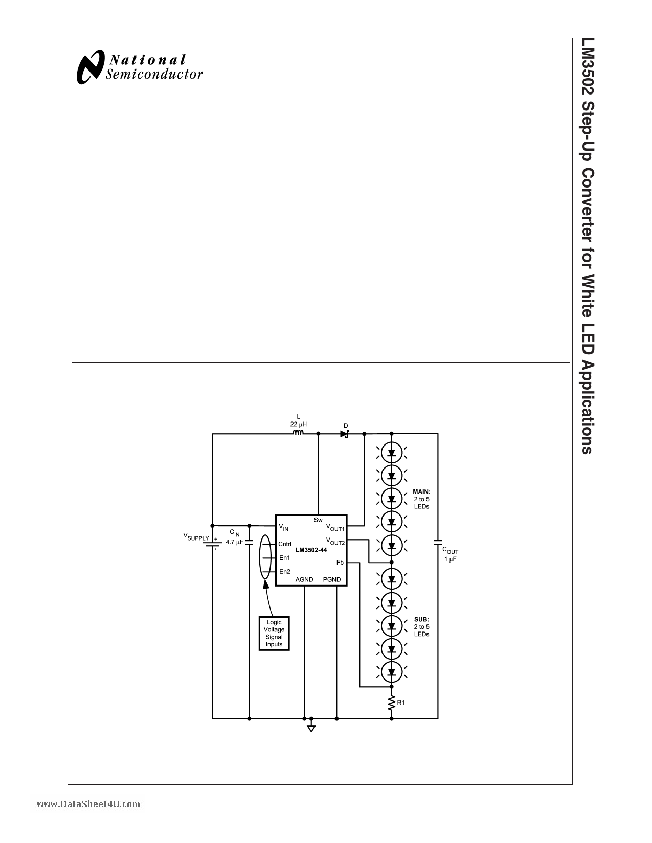
Typical Application
20131701
FIGURE 1. Blacklight Configuration with 10 White LEDs
© 2006 National Semiconductor Corporation DS201317
www.national.com
1 page 
Preliminary Electrical Characteristics (Notes 6, 7) Limits in standard typeface are for TJ = 25˚C.
Limits in bold typeface apply over the full operating junction temperature range (−40˚C ≤ TJ ≤ +125˚C). Unlesws wotwhe.DrwaitsaeSheet4U.com
specified, VIN = 2.5V. (Continued)
Symbol
Parameter
IVOUT1(ON) VOUT1 Pin Bias
Current (Note 3)
IVOUT2
UVP
OVP
VOUT2 Pin Leakage
Current (Note 3)
Under-Voltage
Protection
Over-Voltage
Protection (Note 5)
VEn1
VEn2
VCntrl
TSHDW
IEn1
IEn2
PMOS FET Switch
Enabling Threshold
(Figure 2: P1)
NMOS FET Switch
Enabling Threshold
(Figure 2: N2)
Device Enabling
Threshold
Shutdown Delay Time
En1 Pin Input Bias
Current
En2 Pin Input Bias
Current
Conditions
VOUT1 = 14V, Cntrl = 1.5V (16)
VOUT1 = 23V, Cntrl = 1.5V (25)
VOUT1 = 32V, Cntrl = 1.5V (35)
VOUT1 = 42V, Cntrl = 1.5V (44)
Fb = 0V, Cntrl = 0V, VOUT2 = 42V
On Threshold
Off Threshold
On Threshold (16)
Off Threshold (16)
On Threshold (25)
Off Threshold (25)
On Threshold (35)
Off Threshold (35)
On Threshold (44)
Off Threshold (44)
Off Threshold (Display Lighting)
On Threshold (Display Lighting)
Off Threshold (Display Lighting)
On Threshold (Display Lighting)
Off Threshold
OnThreshold
En1 = 2.5V
En1 = 0V
En2 = 2.5V
En2 = 0V
Min
2.2
14.5
14.0
22.5
21.5
32.0
31.0
40.5
39.0
1.4
1.4
1.4
8
Typ
40
50
50
85
0.1
2.4
2.3
15.5
15
24
23
34
33
42
41
0.8
0.8
0.8
0.8
0.8
0.8
12
7
0.1
7
0.1
Max
80
100
100
140
3
2.5
16.5
16.0
25.5
24.5
35.0
34.0
43.5
42.0
0.3
0.3
0.3
16
14
14
Units
µA
µA
V
V
V
V
V
ms
µA
µA
Note 1: Absolute maximum ratings indicate limits beyond which damage to the device may occur. Electrical characteristic specifications do not apply when
operating the device outside of its rated operating conditions.
Note 2: The human body model is a 100 pF capacitor discharged through a 1.5 kΩ resistor into each pin. The machine model is a 200 pF capacitor discharged
directly into each pin.
Note 3: Current flows into the pin.
Note 4: The maximum allowable power dissipation is a function of the maximum junction temperature, TJ(MAX), the junction-to-ambient thermal resistance, θJA,
and the ambient temperature, TA. See Thermal Properties for the thermal resistance. The maximum allowable power dissipation at any ambient temperature is
calculated using: PD(MAX) = (TJ(MAX) – TA)/θJA. Exceeding the maximum allowable power dissipation will cause excessive die temperature. For more information
on this topic, please refer to Application Note 1187: Leadless Leadframe Package (LLP) and Application Note 1112 (AN1112) for microSMD chip scale package.
Note 5: The on threshold indicates that the LM3502 is no longer switching or regulating LED current, while the off threshold indicates normal operation.
Note 6: All voltages are with respect to the potential at the GND pin.
Note 7: Min and Max limits are guaranteed by design, test, or statistical analysis. Typical numbers are not guaranteed, but do represent the most likely norm.
Note 8: Current flows out of the pin.
5 www.national.com
5 Page 
Typical Performance Characteristics ( Circuit in Figure 1: L = DO1608C-223 and D = MBRM140T3.
Efficiency: η = POUT/PIN = [(VOUT – VFb) * IOUT]/[VIN * IIN]. TA= 25˚C, unless otherwise stated.) (Continued) www.DataSheet4U.com
VOUT1 Pin Current vs VOUT1 Pin Voltage
Power NMOS RDS(ON) (Figure 2: N1) vs VIN
20131719
NMOS RDS(ON) (Figure 2: N2) vs VIN
20131720
PMOS RDS(ON) (Figure 2: P1) vs VIN
20131721
Feedback Voltage vs Temperature
20131722
20131725
11
www.national.com
11 Page | ||
| Páginas | Total 18 Páginas | |
| PDF Descargar | [ Datasheet LM3502.PDF ] | |
Hoja de datos destacado
| Número de pieza | Descripción | Fabricantes |
| LM350 | THREE.TERMINAL ADJUSTABLE POSITIVE VOLTAGE REGULATOR | ON Semiconductor |
| LM350 | 3-Terminal 3A Positive Adjustable Voltage Regulator | Fairchild Semiconductor |
| LM350 | ADJUSTABLE VOLTAGE REGULATORS THREE-TERMINAL 3 A | STMicroelectronics |
| LM350 | THREE-TERMINAL ADJUSTABLE POSITIVE VOLTAGE REGULATOR | Motorola Semiconductors |
| Número de pieza | Descripción | Fabricantes |
| SLA6805M | High Voltage 3 phase Motor Driver IC. |
Sanken |
| SDC1742 | 12- and 14-Bit Hybrid Synchro / Resolver-to-Digital Converters. |
Analog Devices |
|
DataSheet.es es una pagina web que funciona como un repositorio de manuales o hoja de datos de muchos de los productos más populares, |
| DataSheet.es | 2020 | Privacy Policy | Contacto | Buscar |