|
|
|
PDF MAX5080 Data sheet ( Hoja de datos )
| Número de pieza | MAX5080 | |
| Descripción | 1A / 40V / MAXPower Step-Down DC-DC Converters | |
| Fabricantes | Maxim Integrated Products | |
| Logotipo | ||
Hay una vista previa y un enlace de descarga de MAX5080 (archivo pdf) en la parte inferior de esta página. Total 19 Páginas | ||
|
No Preview Available !
19-3656; Rev 1; 2/07
www.DataSheet4U.com
1A, 40V, MAXPower Step-Down
DC-DC Converters
General Description
The MAX5080/MAX5081 are 250kHz PWM step-down
DC-DC converters with an on-chip, 0.3Ω high-side
switch. The input voltage range is 4.5V to 40V for the
MAX5080 and 7.5V to 40V for the MAX5081. The output
is adjustable from 1.23V to 32V and can deliver up to
1A of load current.
Both devices utilize a voltage-mode control scheme for
good noise immunity in the high-voltage switching envi-
ronment and offer external compensation allowing for
maximum flexibility with a wide selection of inductor val-
ues and capacitor types. The switching frequency is
internally fixed at 250kHz and can be synchronized to
an external clock signal through the SYNC input. Light
load efficiency is improved by automatically switching
to a pulse-skip mode.
All devices include programmable undervoltage lock-
out and soft-start. Protection features include cycle-by-
cycle current limit, hiccup-mode output short-circuit
protection, and thermal shutdown. Both devices are
available in a space-saving, high-power (2.7W), 16-pin
TQFN package and are rated for operation over the
-40°C to +125°C temperature range.
Applications
FireWire® Power Supplies
Distributed Power
Automotive
Industrial
FireWire is a registered trademark of Apple Computer, Inc.
VIN
4.5V TO 40V
Features
♦ 4.5V to 40V (MAX5080) or 7.5V to 40V (MAX5081)
Input Voltage Range
♦ 1A Output Current
♦ VOUT Range From 1.23V to 32V
♦ Internal High-Side Switch
♦ Fixed 250kHz Internal Oscillator
♦ Automatic Switchover to Pulse-Skip Mode at
Light Loads
♦ External Frequency Synchronization
♦ Thermal Shutdown and Short-Circuit Protection
♦ Operates Over the -40°C to +125°C Temperature
Range
♦ Space-Saving (5mm x 5mm) High-Power 16-Pin
TQFN Package
Ordering Information
PART
TEMP RANGE
MAX5080ATE -40°C to +125°C
MAX5081ATE -40°C to +125°C
*EP = Exposed pad.
PIN-
PACKAGE
16 TQFN-EP*
16 TQFN-EP*
PKG
CODE
T1655-2
T1655-2
Pin Configurations appear at end of data sheet.
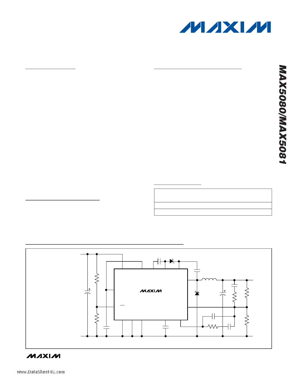
Typical Operating Circuits
CF D1
R1
C1
IN
REG
DVREG C-
C+
BST
LX
MAX5080
ON/OFF
R2 SYNC SGND PGND
C2
PGND
Typical Operating Circuits continued at end of data sheet.
FB
SS COMP
CSS
CBST
L1
D2
VOUT
C6
C5
R6
R3
C8
R5 C7
R4
PGND
________________________________________________________________ Maxim Integrated Products 1
For pricing, delivery, and ordering information, please contact Maxim/Dallas Direct! at
1-888-629-4642, or visit Maxim’s website at www.maxim-ic.com.
1 page 
www.DataSheet4U.com
1A, 40V, MAXPower Step-Down
DC-DC Converters
Typical Operating Characteristics (continued)
(VIN = 12V, see Figure 5 (MAX5080) and Figure 6 (MAX5081), TA = +25°C, unless otherwise noted.)
260
258
256
254
252
250
248
246
244
242
240
-40
OPERATING FREQUENCY
vs. TEMPERATURE
MAXIMUM DUTY CYCLE
vs. INPUT VOLTAGE (MAX5080)
100
MAXIMUM DUTY CYCLE
vs. INPUT VOLTAGE (MAX5081)
100
98 98
96 96
VIN = 4.5V
94
92
94
92
90 90
88 88
VIN = 40V
86
84
86
84
82 82
-15 10 35 60 85 110 135
TEMPERATURE (°C)
80
0
5 10 15 20 25 30 35 40
INPUT VOLTAGE (V)
80
0
5 10 15 20 25 30 35
INPUT VOLTAGE (V)
OPEN-LOOP GAIN/PHASE vs. FREQUENCY
MAX5080 toc10
100 175
80
60
40
20
PHASE
0
GAIN 150
125
100
75
OUTPUT CURRENT LIMIT
vs. INPUT VOLTAGE
2.5
MAX5080
2.4
2.3 TA = -40°C
TA = +25°C
2.2
2.1
2.0
1.9 TA = +85°C TA = +135°C
1.8
1.7
1.6
-20 50
0 0.001 0.01 0.1 1 10 100 1000 10,000
FREQUENCY (kHz)
1.5
0
5 10 15 20 25 30 35 40
INPUT VOLTAGE (V)
40
TURN-ON/OFF WAVEFORM
MAX5080 toc12
ILOAD = 1A
VON/OFF
2V/div
TURN-ON/OFF WAVEFORM
MAX5080 toc13
ILOAD = 100mA
VON/OFF
2V/div
VOUT
2V/div
VOUT
2V/div
2ms/div
2ms/div
_______________________________________________________________________________________ 5
5 Page 
www.DataSheet4U.com
1A, 40V, MAXPower Step-Down
DC-DC Converters
For applications that do not require a 4.5V minimum
input, use the MAX5081. In this device the charge
pump is omitted and the input voltage range is from
7.5V to 40V. In this situation the boost diode and the
boost capacitor are still required (see the MAX5081
Typical Operating Circuit).
Gate Drive Supply (DVREG)
DVREG is the supply input for the internal high-side
MOSFET driver. The power for DVREG is derived from
the output of the internal regulator (REG). Connect
DVREG to REG externally. We recommend the use of
an RC filter (1Ω and 0.47µF) from REG to DVREG to fil-
ter the noise generated by the switching of the charge
pump. In the MAX5080, the high-side drive supply is
generated using the internal charge pump along with
the bootstrap diode and capacitor. In the MAX5081, the
high-side MOSFET driver supply is generated using
only the bootstrap diode and capacitor.
Error Amplifier
The output of the internal error amplifier (COMP) is avail-
able for frequency compensation (see the Compensation
Design section). The inverting input is FB, the noninvert-
ing input SS, and the output COMP. The error amplifier
has an 80dB open-loop gain and a 1.8MHz GBW prod-
uct. See the Typical Operating Character-istics for the
Gain and Phase vs. Frequency graph.
Oscillator/Synchronization Input (SYNC)
With SYNC tied to SGND, the MAX5080/MAX5081 use
their internal oscillator and switch at a fixed frequency
of 250kHz. For external synchronization, drive SYNC
with an external clock from 150kHz to 350kHz. When
driven with an external clock, the device synchronizes
to the rising edge of SYNC.
PWM Comparator/Voltage Feedforward
An internal 250kHz ramp generator is compared
against the output of the error amplifier to generate the
PWM signal. The maximum amplitude of the ramp
(VRAMP) automatically adjusts to compensate for input
voltage and oscillator frequency changes. This causes
the VIN/VRAMP to be a constant 10V/V across the input
voltage range of 4.5V to 40V (MAX5080) or 7.5V to 40V
(MAX5081) and the SYNC frequency range of 150kHz
to 350kHz.
Output Short-Circuit Protection
(Hiccup Mode)
The MAX5080/MAX5081 protects against an output short
circuit by utilizing hiccup-mode protection. In hiccup
mode, a series of sequential cycle-by-cycle current-limit
events will cause the part to shut down and restart with
a soft-start sequence. This allows the device to operate
with a continuous output short circuit.
During normal operation, the current is monitored at the
drain of the internal power MOSFET. When the current
limit is exceeded, the internal power MOSFET turns off
until the next on-cycle and a counter increments. If the
counter counts seven consecutive current-limit events,
the device discharges the soft-start capacitor and
shuts down for 512 clock periods before restarting with
a soft-start sequence. Each time the power MOSFET
turns on and the device does not exceed the current
limit, the counter is reset.
Thermal-Overload Protection
The MAX5080/MAX5081 feature an integrated thermal-
overload protection. Thermal-overload protection limits
the total power dissipation in the device and protects it
in the event of an extended thermal fault condition.
When the die temperature exceeds +160°C, an internal
thermal sensor shuts down the part, turning off the
power MOSFET and allowing the IC to cool. After the
temperature falls by 20°C, the part will restart with a
soft-start sequence.
Applications Information
Setting the Undervoltage Lockout
When the voltage at ON/OFF rises above 1.23V, the
MAX5080/MAX5081 turns on. Connect a resistive
divider from IN to ON/OFF to SGND to set the UVLO
threshold (see Figure 5). First select the ON/OFF to the
SGND resistor (R2) then calculate the resistor from IN
to ON/OFF (R1) using the following equation:
R1 = R2 ×
⎡
⎢
⎣⎢
VIN
VON/OFF
⎤
− 1⎥
⎦⎥
where VIN is the input voltage at which the converter
turns on, VON/OFF = 1.23V and R2 is chosen to be less
than 600kΩ.
If the external UVLO divider is not used, connect
ON/OFF to IN directly. In this case, an internal under-
voltage lockout feature monitors the supply voltage at
IN and allows operation to start when IN rises above
4.1V (MAX5080) and 7.1V (MAX5081).
Setting the Output Voltage
Connect a resistive divider from OUT to FB to SGND to
set the output voltage. First calculate the resistor from
OUT to FB using the guidelines in the Compensation
Design section. Once R3 is known, calculate R4 using
the following equation:
______________________________________________________________________________________ 11
11 Page | ||
| Páginas | Total 19 Páginas | |
| PDF Descargar | [ Datasheet MAX5080.PDF ] | |
Hoja de datos destacado
| Número de pieza | Descripción | Fabricantes |
| MAX5080 | 1A / 40V / MAXPower Step-Down DC-DC Converters | Maxim Integrated Products |
| MAX5081 | 1A / 40V / MAXPower Step-Down DC-DC Converters | Maxim Integrated Products |
| MAX5082 | 1.5A / 40V / MAXPower Step-Down DC-DC Converters | Maxim Integrated Products |
| MAX5083 | 1.5A / 40V / MAXPower Step-Down DC-DC Converters | Maxim Integrated Products |
| Número de pieza | Descripción | Fabricantes |
| SLA6805M | High Voltage 3 phase Motor Driver IC. |
Sanken |
| SDC1742 | 12- and 14-Bit Hybrid Synchro / Resolver-to-Digital Converters. |
Analog Devices |
|
DataSheet.es es una pagina web que funciona como un repositorio de manuales o hoja de datos de muchos de los productos más populares, |
| DataSheet.es | 2020 | Privacy Policy | Contacto | Buscar |