|
|
|
PDF AD6636 Data sheet ( Hoja de datos )
| Número de pieza | AD6636 | |
| Descripción | 150 MSPS Wideband Digital Down-Converter (DDC) | |
| Fabricantes | Analog Devices | |
| Logotipo | ||
Hay una vista previa y un enlace de descarga de AD6636 (archivo pdf) en la parte inferior de esta página. Total 30 Páginas | ||
|
No Preview Available !
150 MSPS Wideband
www.DataSheet4U.com
Digital Down-Converter (DDC)
AD6636
FEATURES
4/6 independent wideband processing channels
Processes 6 wideband carriers (UMTS, CDMA2000)
4 single-ended or 2 LVDS parallel input ports
(16 linear bit plus 3-bit exponent) running at 150 MHz
Supports 300 MSPS input using external interface logic
3 16-bit parallel output ports operating up to 200 MHz
Real or complex input ports
Quadrature correction and dc correction for complex inputs
Supports output rate up to 34 MSPS per channel
RMS/peak power monitoring of input ports
Programmable attenuator control for external gain ranging
3 programmable coefficient FIR filters per channel
2 decimating half-band filters per channel
6 programmable digital AGC loops with 96 dB range
Synchronous serial I/O operation (SPI®-, SPORT-compatible)
Supports 8-bit or 16-bit microport modes
3.3 V I/O, 1.8 V CMOS core
User-configurable built-in self-test (BIST) capability
JTAG boundary scan
APPLICATIONS
Multicarrier, multimode digital receivers
GSM, EDGE, PHS, UMTS, WCDMA, CDMA2000, TD-SCDMA
Micro and pico cell systems, software radios
Broadband data applications
Instrumentation and test equipment
Wireless local loop
In-building wireless telephony
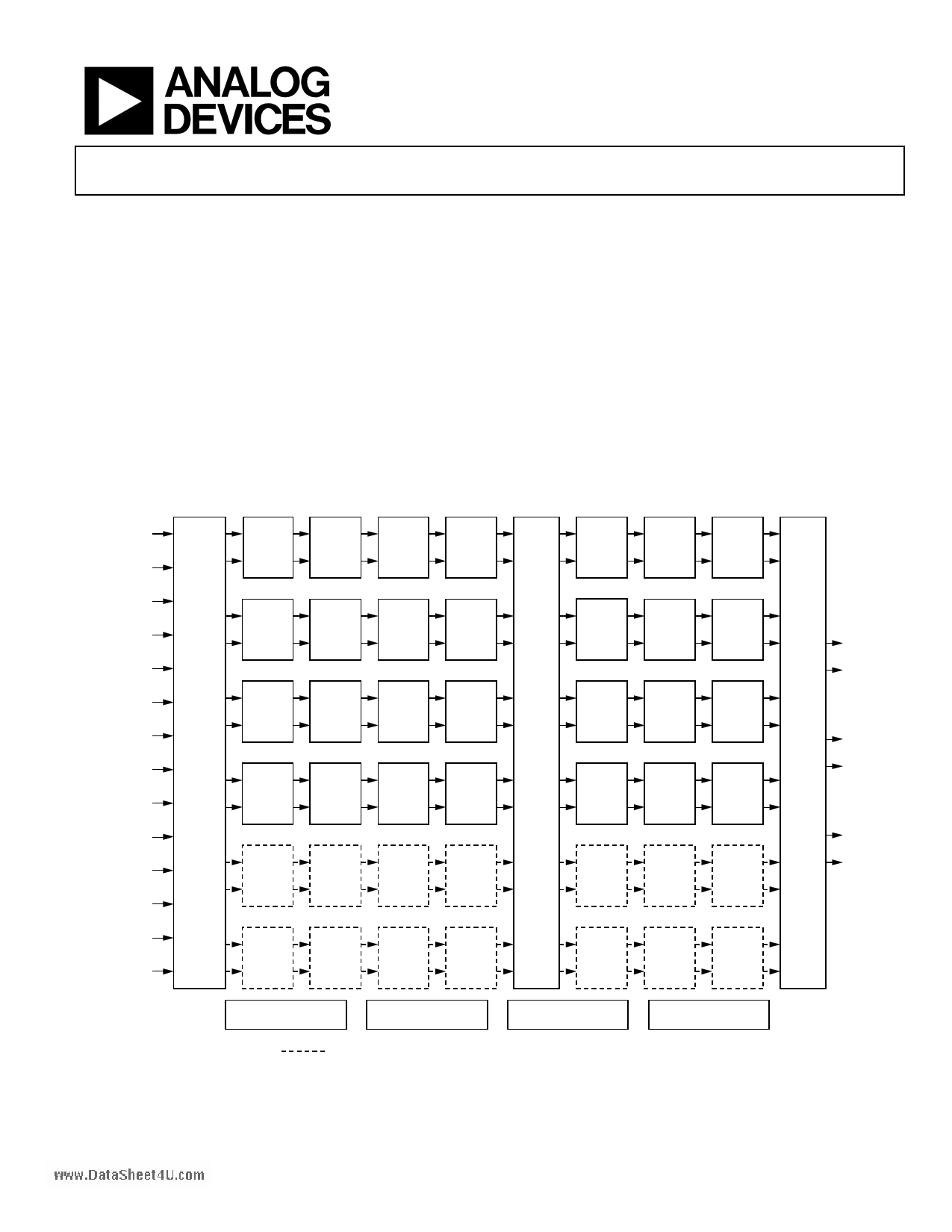
FUNCTIONAL BLOCK DIAGRAM
CLKA
ADC A/AI
NCO
CIC5
M = 1-32
FIR1
HB1
M = Byp, 2
FIR2
HB2
M = Byp, 2
MRCF
DRCF
M = 1-16
CRCF
M = 1-16
LHB
L = Byp, 2
EXPA [2:0]
CLKB
ADC B/AQ
EXPB [2:0]
CLKC
ADC C/CI
CMOS
REAL
PORTS
A, B,
C,D
CMOS
EXPC [2:0] COMPLEX
PORTS
(AI, AQ)
CLKD (BI, BQ)
ADC D/CQ
EXPD [2:0]
______
RESET
SYNC [3:0]
LVDS
PORTS
AB, CD
PEAK/
RMS
MEAS.
I,Q
CORR.
NCO
NCO
NCO
NCO
NCO
CIC5
M = 1-32
FIR1
HB1
M = Byp, 2
FIR2
HB2
M = Byp, 2
CIC5
M = 1-32
FIR1
HB1
M = Byp, 2
FIR2
HB2
M = Byp, 2
CIC5
M = 1-32
FIR1
HB1
M = Byp, 2
FIR2
HB2
M = Byp, 2
CIC5
M = 1-32
FIR1
HB1
M = Byp, 2
FIR2
HB2
M = Byp, 2
CIC5
M = 1-32
FIR1
HB1
M = Byp, 2
FIR2
HB2
M = Byp, 2
MRCF
DRCF
M = 1-16
CRCF
M = 1-16
LHB
L = Byp, 2
PA
MRCF
DRCF
M = 1-16
CRCF
M = 1-16
LHB
L = Byp, 2
MRCF
DRCF
M = 1-16
CRCF
M = 1-16
LHB
L = Byp, 2
AGC PB
MRCF
DRCF
M = 1-16
CRCF
M = 1-16
LHB
L = Byp, 2
PC
MRCF
DRCF
M = 1-16
CRCF
M = 1-16
LHB
L = Byp, 2
PLL CLOCK
MULTIPLIER
16-BIT
MICROPORT INTERFACE
SPORT/SPI INTERFACE
JTAG
NOTE: CHANNELS RENDERED AS
ARE AVAILABLE ONLY IN 6-CHANNEL PART
M = DECIMATION
L = INTERPOLATION
Figure 1.
Rev. 0
Information furnished by Analog Devices is believed to be accurate and reliable.
However, no responsibility is assumed by Analog Devices for its use, nor for any
infringements of patents or other rights of third parties that may result from its use.
Specifications subject to change without notice. No license is granted by implication
or otherwise under any patent or patent rights of Analog Devices. Trademarks and
registered trademarks are the property of their respective owners.
One Technology Way, P.O. Box 9106, Norwood, MA 02062-9106, U.S.A.
Tel: 781.329.4700
www.analog.com
Fax: 781.326.8703 © 2004 Analog Devices, Inc. All rights reserved.
1 page 
SPECIFICATIONS
Table 1. Recommended Operating Conditions
Parameter
Temp
VDDCORE
Full
VDDIO
Full
TAMBIENT
Full
Test Level
IV
IV
IV
Min
1.7
3.0
−40
ELECTRICAL CHARACTERISTICS
Table 2. Electrical Characteristics1
Parameter
LOGIC INPUTS (NOT 5 V TOLERANT)
Logic Compatibility
Logic 1 Voltage
Logic 0 Voltage
Logic 1 Current
Logic 0 Current
Input Capacitance
LOGIC OUTPUTS
Logic Compatibility
Logic 1 Voltage (IOH = 0.25 mA)
Logic 0 Voltage (IOL = 0.25 mA)
SUPPLY CURRENTS
WCDMA (61.44 MHz) Example1
IVDDCORE
IVDDIO
CDMA 2000 (61.44 MHz) Example1
IVDDCORE
IVDDIO
TDS-CDMA (76.8 MHz) Example1, 2
IVDDCORE
IVDDIO
GSM (65 MHz) Example1, 2
IVDDCORE
IVDDIO
TOTAL POWER DISSIPATION
WCDMA (61.44 MHz)1
CDMA 2000 (61.44 MHz)1
TDS-CDMA, (76.8 MHz)1, 2
GSM, (65 MHz)1, 2
Temp
Full
Full
Full
Full
Full
25°C
Full
Full
Full
25°C
25°C
25°C
25°C
25°C
25°C
25°C
25°C
25°C
25°C
25°C
25°C
25°C
Test Level
IV
IV
IV
IV
IV
V
IV
IV
IV
V
V
V
V
V
V
V
V
V
V
V
V
V
1 One input port, all six channels, and the relevant signal processing blocks are active.
2 PLL is turned off for power savings.
Min
3.3
2.0
−0.3
3.3
2.0
AD6636www.DataSheet4U.com
Typ Max Unit
1.8 1.9 V
3.3 3.6 V
+25 +85 °C
Typ Max Unit
V CMOS
3.6 V
+0.8 V
1 10 µA
1 10 µA
4 pF
VDDIO − 0.2
0.2
0.4
V CMOS
V
V
450 mA
50 mA
400 mA
25 mA
250 mA
15 mA
175 mA
10 mA
975 mW
800 mW
500 mW
350 mW
Rev. 0 | Page 5 of 72
5 Page 
AD6636w w w . D a t a S h e
Name
CLKC, CLKD
INA[0:15], INB[0:15]
Type
Input
LVDS Input
Pin No.
A6, A5
See Table 8
INC[0:15], IND[0:15] LVDS Input See Table 8
OUTPUT PORTS
PCLK
PA[0:15]
PACH[0:2]
PAIQ
PAGAIN
Bidirectional
Output
Output
Output
Output
E16
See Table 8
G15, D16, H12
H13
G13
PAACK
PAREQ
PB[0:15]
PBCH[0:2]
PBIQ
PBGAIN
Input
Output
Output
Output
Output
Output
H14
F15
See Table 8
C13, D11, B14
D12
A14
PBACK
PBREQ
PC[0:15]
PCCH[0:2]
PCIQ
PCGAIN
Input
Output
Output
Output
Output
Output
E12
E11
See Table 8
M15, L14, N15
P15
P16
PCACK
PCREQ
MISC PINS
RESET
IRP
SYNC[0:3]
Input
Output
Input
Output
Input
LVDS_RSET
Input
EXT_FILTER
Input
MICROPORT CONTROL
D[0:15]
Bidirectional
A[0:7]
Input
DS(RD)
Input
L13
R16
P3
T2
B12, A12, C10,
B11
E4
R4
See Table 8
See Table 8
P4
DTACK (RDY)1
Output
M6
R/W (WR)
Input
N4
MODE
Input
T3
CS
CPUCLK
CHIPID[0:3]
Input
Input
Input
N5
R1
T4, R5, N6, P6
Function
LVDS Differential Clock for LVDS_C Input Port (LVDS_CLKC+, LVDS_CLKC−).
In LVDS input mode, INA[0 :15] and INB[0 :15] form a differential pair
LVDS_A+[0:15] (positive node) and LVDS_A–[0:15] (negative node), respectively.
In LVDS input mode, INC[0 :15] and IND[0 :15] form a differential pair
LVDS_C+[0:15] (positive node) and LVDS_C–[0:15] (negative node), respectively.
Parallel Output Port Clock. Master mode output, Slave mode input.
Parallel Output Port A Data Bus.
Channel Indicator Output Port A.
Parallel Port A I/Q Data Indicator. Logic 1 indicates I data on data bus.
Parallel Port A Gain Word Output Indicator. Logic 1 indicates gain word on
data bus.
Parallel Port A Acknowledge (Active High).
Parallel Port A Request (Active High).
Parallel Output Port B Data Bus.
Channel Indicator Output Port B.
Parallel Port B I/Q Data Indicator. Logic 1 indicates I data on data bus.
Parallel Port B Gain Word Output Indicator. Logic 1 indicates gain word on
data bus.
Parallel Port B Acknowledge (Active High).
Parallel Port B Request (Active High).
Parallel Output Port C Data Bus.
Channel Indicator Output Port C.
Parallel Port C I/Q Data Indicator. Logic 1 indicates I data on data bus.
Parallel Port C Gain Word Output Indicator. Logic 1 indicates gain word on
data bus.
Parallel Port C Acknowledge (Active High).
Parallel Port C Request (Active High).
Master Reset (Active Low).
Interrupt Pin.
Synchronization Inputs. SYNC pins are independent of channels or input ports and
independent of each other.
LVDS Resistor Set Pin (Analog Pin). See Design Notes.
PLL Loop Filter (Analog Pin). See Design Notes.
Bidirectional Microport Data. This bus is three-stated when CS is high.
Microport Address Bus.
Active Low Data Strobe when MODE = 1.
Active Low Read Strobe when MODE = 0.
Active Low Data Acknowledge when MODE = 1.
Microport Status Pin when MODE = 0.
Read/Write Strobe when MODE = 1.
Active Low Write Strobe when MODE = 0.
Mode Select Pin.
When SMODE = 0: Logic 0 = Intel mode; Logic 1 = Motorola mode.
When SMODE = 1: Logic 0 = SPI mode; Logic 1 = SPORT mode.
Active Low Chip Select. Logic 1 three-states the microport data bus.
Microport CLK Input (Input Only).
Chip ID Input Pins.
Rev. 0 | Page 11 of 72
11 Page | ||
| Páginas | Total 30 Páginas | |
| PDF Descargar | [ Datasheet AD6636.PDF ] | |
Hoja de datos destacado
| Número de pieza | Descripción | Fabricantes |
| AD6630 | Differential/ Low Noise IF Gain Block with Output Clamping | Analog Devices |
| AD6633 | Multichannel Digital Upconverter | Analog Devices |
| AD6634 | 80 MSPS/ Dual-Channel WCDMA Receive Signal Processor (RSP) | Analog Devices |
| AD6635 | 4-Channel/ 80 MSPS WCDMA Receive Signal Processor (RSP) | Analog Devices |
| Número de pieza | Descripción | Fabricantes |
| SLA6805M | High Voltage 3 phase Motor Driver IC. |
Sanken |
| SDC1742 | 12- and 14-Bit Hybrid Synchro / Resolver-to-Digital Converters. |
Analog Devices |
|
DataSheet.es es una pagina web que funciona como un repositorio de manuales o hoja de datos de muchos de los productos más populares, |
| DataSheet.es | 2020 | Privacy Policy | Contacto | Buscar |