|
|
|
PDF AD8155 Data sheet ( Hoja de datos )
| Número de pieza | AD8155 | |
| Descripción | 6.5 Gbps Dual Buffer Mux/Demux | |
| Fabricantes | Analog Devices | |
| Logotipo | ||
Hay una vista previa y un enlace de descarga de AD8155 (archivo pdf) en la parte inferior de esta página. Total 30 Páginas | ||
|
No Preview Available !
www.DataSheet4U.com
FEATURES
Dual 2:1 mux/1:2 demux
Optimized for dc to 6.5 Gbps NRZ data
Per-lane P/N pair inversion for routing ease
Programmable input equalization
Compensates up to 40 inches of FR4
Loss-of-signal detection
Programmable output preemphasis up to 12 dB
Programmable output levels with squelch and disable
Accepts ac-coupled or dc-coupled differential CML inputs
50 Ω on-chip termination
1:2 demux supports unicast or bicast operation
Port-level loopback
Port or single lane switching
1.8 V to 3.3 V flexible core supply
User-settable I/O supply from VCC to 1.2 V
Low power, typically 2.0 W in basic configuration
64-lead LFCSP
−40°C to +85°C operating temperature range
APPLICATIONS
Low cost redundancy switch
SONET OC48/SDH16 and lower data rates
RXAUI, 4× Fibre Channel, Infiniband, and GbE over
backplane
OIF CEI 6.25 Gbps over backplane
Serial data-level shift
2-/4-/6-lane equalizers or redrivers
GENERAL DESCRIPTION
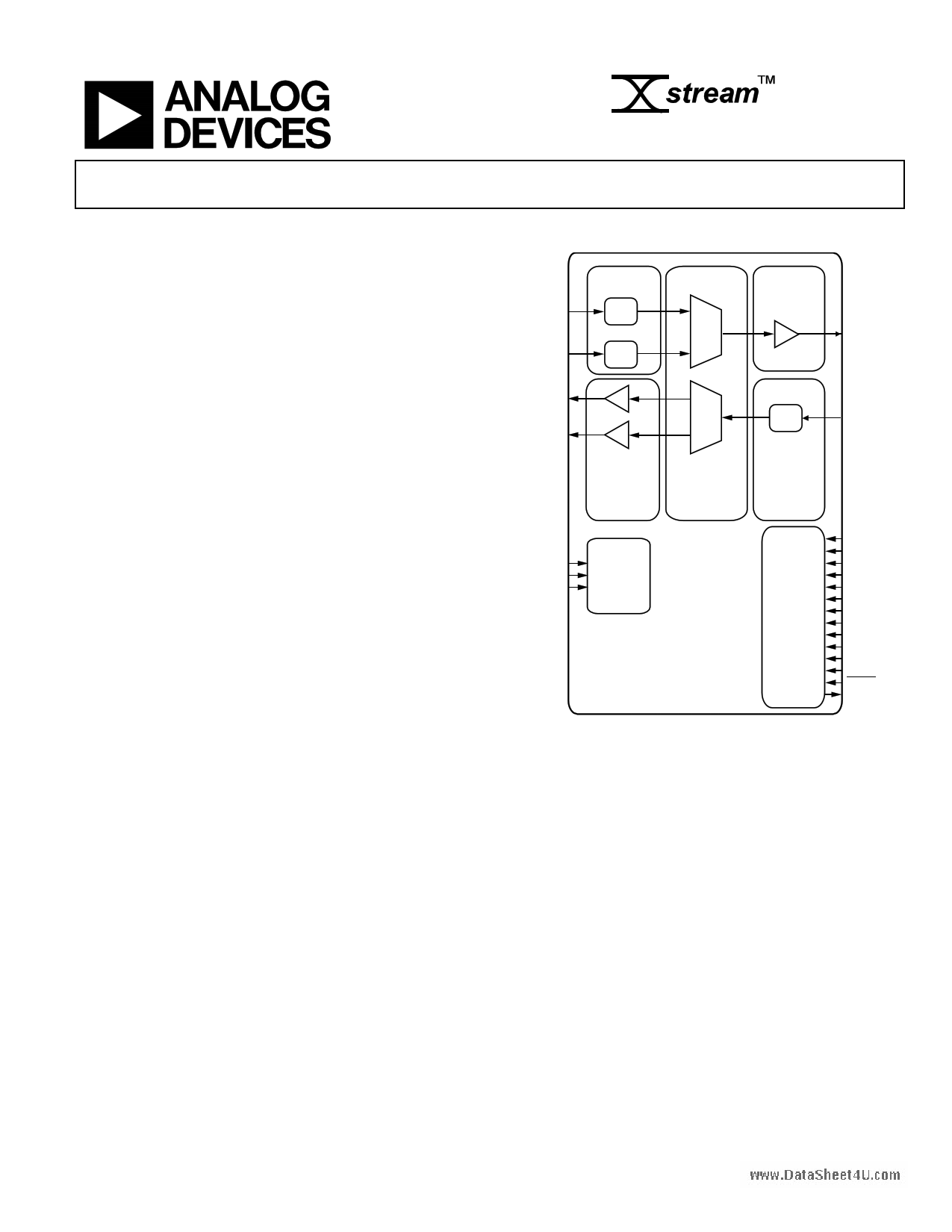
The AD8155 is an asynchronous, protocol-agnostic, dual-lane
2:1 switch with a total of six differential CML inputs and
six differential CML outputs. The signal path supports NRZ
signaling with data rates up to 6.5 Gbps per lane. Each lane
offers programmable receive equalization, programmable
output preemphasis, programmable output levels, and loss-of-
signal detection.
The nonblocking switch core of the AD8155 implements a
2:1 multiplexer and 1:2 demultiplexer per lane and supports
independent lane switching through the two select pins,
SEL[1:0]. Each port is a two-lane link. Every lane implements
an asynchronous path supporting dc to 6.5 Gbps NRZ data,
fully independent of other lanes. The AD8155 has low latency
and very low lane-to-lane skew.
Rev. 0
Information furnished by Analog Devices is believed to be accurate and reliable. However, no
responsibility is assumed by Analog Devices for its use, nor for any infringements of patents or other
rights of third parties that may result from its use. Specifications subject to change without notice. No
license is granted by implication or otherwise under any patent or patent rights of Analog Devices.
Trademarksandregisteredtrademarksarethepropertyoftheirrespectiveowners.
6.5 Gbps
Dual Buffer Mux/Demux
AD8155
FUNCTIONAL BLOCK DIAGRAM
Ix_A[1:0]
RECEIVE
EQUALIZATION
EQ
Ix_B[1:0]
EQ
2:1
TRANSMIT
PRE-
EMPHASIS
Ox_C[1:0]
Ox_A[1:0]
Ox_B[1:0]
SCL
SDA
I2C_A[2:0]
1:2 EQ Ix_C[1:0]
TRANSMIT
PRE-
EMPHASIS
DUAL
2:1
MULTIPLEXER/
1:2
DEMULTIPLEXER
RECEIVE
EQUALIZATION
I2C
CONTROL
LOGIC
AD8155
CONTROL
LOGIC
LB_A
LB_B
LB_C
PE_A
PE_B
PE_C
EQ_A
EQ_B
EQ_C
SEL[1:0]
BICAST
SEL4G
RESET
LOS_INT
Figure 1.
The main application of the AD8155 is to support redundancy
on both the backplane and the line interface sides of a serial
link. The demultiplexing path implements unicast and bicast
capability, allowing the part to support either 1 + 1 or 1:1
redundancy.
The AD8155 is also suited for testing high speed serial links
because of its ability to duplicate incoming data. In a port-
monitoring application, the AD8155 can maintain link
connectivity with a pass-through connection from Port C to
Port A while sending a duplicate copy of the data to test
equipment on Port B.
The rich feature set of the AD8155 can be controlled either
through external toggle pins or by setting on-chip control
registers through the I2C® interface.
One Technology Way, P.O. Box 9106, Norwood, MA 02062-9106, U.S.A.
Tel: 781.329.4700
www.analog.com
Fax: 781.461.3113
©2009 Analog Devices, Inc. All rights reserved.
1 page 
www.DataSheet4U.com
AD8155
I2C TIMING SPECIFICATIONS
SDA
tF tLOW
SCL
tHD;STA
S
NOTES
1. S = START CONDITION.
2. Sr = REPEAT START.
3. P = STOP.
tR tSU;DAT
tHD;DAT
tHIGH
Table 2. I2C Timing Parameters
Parameter
SCL Clock Frequency
Hold Time for a Start Condition
Setup Time for a Repeated Start Condition
Low Period of the SCL Clock
High Period of the SCL Clock
Data Hold Time
Data Setup Time
Rise Time for Both SDA and SCL
Fall Time for Both SDA and SCL
Setup Time for Stop Condition
Bus Free Time Between a Stop and a Start Condition
Bus Free Time After a Reset
Reset Pulse Width
Capacitance for Each I/O Pin
tF
tHD;STA
tR tBUF
tSU;STA
Sr
tSU;STO
P
S
Figure 2. I2C Timing Diagram
Symbol
fSCL
tHD;STA
tSU;STA
tLOW
tHIGH
tHD;DAT
tSU;DAT
tR
tF
tSU;STO
tBUF
Ci
Min Max
0 400+
0.6
0.6
1.3
0.6
0
10
1 300
1 300
0.6
1
1
10
57
Unit
kHz
μs
μs
μs
μs
μs
ns
ns
ns
μs
μs
μs
ns
pF
Rev. 0 | Page 5 of 36
5 Page 
www.DataSheet4U.com
AD8155
50Ω CABLES
50Ω CABLES
50Ω CABLES
DATA OUT 2
2 INPUT OUTPUT 2
PIN PIN
2 FR4 TEST BACKPLANE 2
2
50Ω
PATTERN
GENERATOR
AD8155
TP1 AC-COUPLED
EVALUATION
BOARD
DIFFERENTIAL
TP2
STRIPLINE TRACES
8mils WIDE, 8mils SPACE,
8mils DIELECTRIC HEIGHT
HIGH
TP3
SPEED
SAMPLING
OSCILLOSCOPE
TRACE LENGTHS = 20 INCHES,
30 INCHES
25ps/DIV
REFERENCE EYE DIAGRAM AT TP1
Figure 12. Output Preemphasis Test Circuit
25ps/DIV
Figure 13. 6.5 Gbps Output Eye, 20 Inch FR4 Input Channel, PE = 0
(TP3 from Figure 12)
25ps/DIV
Figure 15. 6.5 Gbps Output Eye, 20 Inch FR4 Input Channel, PE = Best Setting,
Default Output Level (TP3 from Figure 12)
25ps/DIV
Figure 14. 6.5 Gbps Output Eye, 30 Inch FR4 Input Channel, PE = 0
(TP3 from Figure 12)
25ps/DIV
Figure 16. 6.5 Gbps Output Eye, 30 Inch FR4 Input Channel, PE = Best Setting,
200 mV Output Level (TP3 from Figure 12)
Rev. 0 | Page 11 of 36
11 Page | ||
| Páginas | Total 30 Páginas | |
| PDF Descargar | [ Datasheet AD8155.PDF ] | |
Hoja de datos destacado
| Número de pieza | Descripción | Fabricantes |
| AD815 | High Output Current Differential Driver | Analog Devices |
| AD8150 | 33 x 17/ 1.5 Gbps Digital Crosspoint Switch | Analog Devices |
| AD8151 | Digital Crosspoint Switch | Analog Devices |
| AD8152 | Digital Crosspoint Switch | Analog Devices |
| Número de pieza | Descripción | Fabricantes |
| SLA6805M | High Voltage 3 phase Motor Driver IC. |
Sanken |
| SDC1742 | 12- and 14-Bit Hybrid Synchro / Resolver-to-Digital Converters. |
Analog Devices |
|
DataSheet.es es una pagina web que funciona como un repositorio de manuales o hoja de datos de muchos de los productos más populares, |
| DataSheet.es | 2020 | Privacy Policy | Contacto | Buscar |