|
|
|
PDF MAX2034 Data sheet ( Hoja de datos )
| Número de pieza | MAX2034 | |
| Descripción | Ultra-Low-Noise Amplifier | |
| Fabricantes | Maxim Integrated Products | |
| Logotipo | ||
1. MAX2034 Hay una vista previa y un enlace de descarga de MAX2034 (archivo pdf) en la parte inferior de esta página. Total 13 Páginas | ||
|
No Preview Available !
19-3969; Rev 1; 3/07
www.DataSheet4U.com
Quad-Channel, Ultra-Low-Noise Amplifier with
Digitally Programmable Input Impedance
General Description
The MAX2034 four-channel, low-power, ultra-low-noise
preamplifier is designed for ultrasound and medical
instrumentation applications. Each low-noise amplifier
has a single-ended input, differential output, a highly
accurate 19dB fixed gain, and a wide -3dB bandwidth
of 70MHz. The high-gain accuracy of the amplifier
allows for exceptional channel-to-channel gain match-
ing, which is necessary for high-performance ultra-
sound-imaging applications. The MAX2034 also
includes an on-chip programmable input impedance
feature that allows the device to be compatible with a
variety of common source impedances ranging from
50Ω to 1kΩ. The input impedance of each amplifier
uses a feedback topology for active impedance match-
ing. The active input impedance matching feature
achieves an exceptionally low 2.2dB noise figure with a
source and input impedance of 200Ω.
The MAX2034 has excellent dynamic and linearity per-
formance characteristics optimized for all ultrasound-
imaging modalities including second harmonic 2D
imaging and continuous wave Doppler. The device
achieves a second harmonic distortion of -68dBc at
VOUT = 1VP-P and fIN = 5MHz, and an ultrasound-spe-
cific* two-tone third-order intermodulation distortion per-
formance of -55dBc at VOUT = 1VP-P and fIN = 5MHz.
The MAX2034 is also optimized for quick overload
recovery for operation under the large input signal con-
ditions typically found in ultrasound input-buffer imag-
ing applications.
The MAX2034 is available in a 48-pin thin QFN pack-
age with an exposed paddle. Electrical performance is
guaranteed over a 0°C to +70°C temperature range.
Ordering Information
PART
TEMP
RANGE
PIN-
PACKAGE
PKG
CODE
MAX2034CTM+ 0°C to +70°C 48 Thin QFN-EP** T4877-4
(7mm x 7mm)
MAX2034CTM
0°C to +70°C
48 Thin QFN-EP**
(7mm x 7mm)
T4877-4
MAX2034CTM+T 0°C to +70°C 48 Thin QFN-EP** T4877-4
(7mm x 7mm)
MAX2034CTM-T 0°C to +70°C 48 Thin QFN-EP** T4877-4
(7mm x 7mm)
**EP = Exposed paddle.
+Denotes lead-free package.
T = Tape-and-reel package.
*See the Ultrasound-Specific IMD3 Specification in the
Applications Information section.
Features
♦ High-Level Integration of 4 Channels
♦ Digitally Programmable Input Impedance (RIN) of
50Ω, 100Ω, 200Ω, and 1kΩ
♦ Integrated Input Clamp
♦ Integrated Input-Damping Capacitor
♦ Ultra-Low 2.2dB Noise Figure at RS = RIN = 200Ω
♦ 70MHz, -3dB Bandwidth
♦ Low 58mW/Channel Power Dissipation
♦ HD2 of -68dBc at VOUT = 1VP-P and fIN = 5MHz for
Exceptional Second Harmonic Imaging
Performance
♦ Two-Tone Ultrasound-Specific* IMD3 of -55dBc at
VOUT = 1VP-P and fIN = 5MHz for Exceptional
PW/CW Doppler Performance
♦ Quick Large-Signal Overload Recovery
♦ Single +5V Supply Operation
♦ Sleep Mode
Applications
Ultrasound Imaging
Sonar Signal Amplification
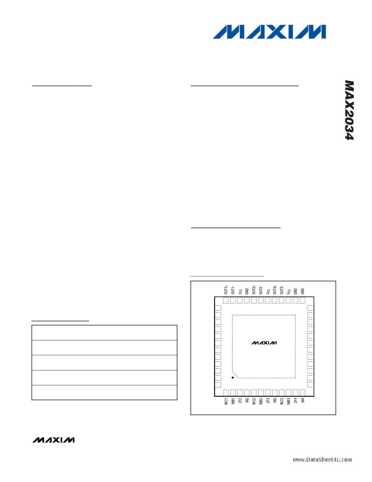
Pin Configuration
TOP VIEW
36 35 34 33 32 31 30 29 28 27 26 25
GND 37
VCC 38
GND 39
GND 40
24 OUT4+
23 OUT4-
22 GND
21 GND
VCC 41
D2 42
PD 43
VCC 44
VCC 45
GND 46
ZF1 47
IN1 48
MAX2034
20 VCC
19 D0
18 D1
17 VCC
16 VCC
15 GND
14 INB4
13 INC4
1 2 3 4 5 6 7 8 9 10 11 12
THIN QFN
Typical Application Circuit appears at end of data sheet.
________________________________________________________________ Maxim Integrated Products 1
For pricing, delivery, and ordering information, please contact Maxim/Dallas Direct! at
1-888-629-4642, or visit Maxim’s website at www.maxim-ic.com.
1 page 
www.DataSheet4U.com
Quad-Channel, Ultra-Low-Noise Amplifier with
Digitally Programmable Input Impedance
Typical Operating Characteristics (continued)
(MAX2034 Typical Application Circuit, VCC = +4.75V to +5.25V, source impedance RS = 200Ω, PD = 0, D2/D1/D0 = 0/1/0 (RIN = 200Ω),
signal AC-coupled to IN_, INB_ is AC grounded, VOUT is the differential output between OUT_+ and OUT_-, fIN_ = 5MHz, RL = 200Ω
between the differential outputs, CL = 20pF from each output to ground, TA = 0°C to +70°C, unless otherwise specified.)
TWO-TONE ULTRASOUND-SPECIFIC IMD3
vs. FREQUENCY
0
VOUT = 1VP-P DIFFERENTIAL
-10 RL = 200Ω
-20
-30
-40
-50
-60
LARGE-SIGNAL NOISE FIGURE
vs. OFFSET FREQUENCY
6
RIN = 200Ω
5
RL = 200Ω
fIN_ = 5MHz
4 VIN = 300mVP-P
3 VIN = 200mVP-P
2
VIN = 112mVP-P
1
SMALL-SIGNAL
NOISE FIGURE
-70
0
5 10 15 20 25 30
FREQUENCY (MHz)
GAIN-ERROR HISTOGRAM
50
SAMPLE SIZE = 243 UNITS
45 fIN_ = 5MHz, VIN = 112mVP-P
40
35
30
25
20
15
10
5
0
GAIN ERROR (dB)
SUPPLY CURRENT
vs. DIFFERENTIAL OUTPUT VOLTAGE
130
ALL CHANNELS ACTIVE
0
0.1 1 10
OFFSET FREQUENCY (kHz)
100
CHANNEL-TO-CHANNEL CROSSTALK
vs. FREQUENCY
-30
VOUT = 1VP-P DIFFERENTIAL
-40 RL = 200Ω
ADJACENT CHANNELS
-50
-60
-70
-80
-90
-100
1
10
FREQUENCY (MHz)
100
LARGE-SIGNAL RECOVERY
MAX2034 toc15
fIN_ = 5MHz
110
90 RL = 200Ω
70
NO LOAD
50
INPUT IN_
500mV/div
DIFFERENTIAL
OUTPUT
OUT_+ - OUT_-
2.0V/div
30
0
123
DIFFERENTIAL OUTPUT VOLTAGE (VP-P)
4
400ns/div
_______________________________________________________________________________________ 5
5 Page 
www.DataSheet4U.com
Quad-Channel, Ultra-Low-Noise Amplifier with
Digitally Programmable Input Impedance
Typical 200Ω Application Circuit
100nF
18nF
+5V
100nF
100nF
RS = 200Ω
100nF
RS = 200Ω
100nF
100nF
RS = 200Ω
100nF
100nF
RS = 200Ω
100nF
18nF
18nF
18nF
INC1
1
INB1
2
ZF2
3
IN2
4
INC2
5
INB2
6
ZF3
7
IN3
8
INC3
9
INB3 10
ZF4
11
IN4
12
48 47 46 45 44 43 42 41 40 39 38 37
MAX2034
EXPOSED PADDLE
OUT1+
36
OUT1-
35
VCC
34
GND
33
OUT2+
32
OUT2-
31
30 VCC
OUT3+
29
OUT3-
28
27 VCC
26 GND
25 GND
13 14 15 16 17 18 19 20 21 22 23 24
100nF
100nF
100nF
100nF
100nF
100nF
100nF
100nF
100nF
100nF
100nF
+5V +5V
100nF
100nF
100nF
______________________________________________________________________________________ 11
11 Page | ||
| Páginas | Total 13 Páginas | |
| PDF Descargar | [ Datasheet MAX2034.PDF ] | |
Hoja de datos destacado
| Número de pieza | Descripción | Fabricantes |
| MAX203 | +5V-Powered / Multichannel RS-232 Drivers/Receivers | Maxim Integrated |
| MAX2031 | 815MHz to 1000MHz Upconversion/ Downconversion Mixer | Maxim Integrated Products |
| MAX2032 | 650MHz to 1000MHz Upconversion/Downconversion Mixer | Maxim Integrated Products |
| MAX2034 | Ultra-Low-Noise Amplifier | Maxim Integrated Products |
| Número de pieza | Descripción | Fabricantes |
| SLA6805M | High Voltage 3 phase Motor Driver IC. |
Sanken |
| SDC1742 | 12- and 14-Bit Hybrid Synchro / Resolver-to-Digital Converters. |
Analog Devices |
|
DataSheet.es es una pagina web que funciona como un repositorio de manuales o hoja de datos de muchos de los productos más populares, |
| DataSheet.es | 2020 | Privacy Policy | Contacto | Buscar |