|
|
|
PDF ISL22317 Data sheet ( Hoja de datos )
| Número de pieza | ISL22317 | |
| Descripción | Precision Single Digitally Controlled Potentiometer | |
| Fabricantes | Intersil Corporation | |
| Logotipo | ||
Hay una vista previa y un enlace de descarga de ISL22317 (archivo pdf) en la parte inferior de esta página. Total 15 Páginas | ||
|
No Preview Available !
www.DataSheet4U.com
ISL22317
® Precision Single Digitally Controlled Potentiometer (XDCP™)
Data Sheet
May 26, 2009
FN6912.0
Low Noise, Low Power, I2C™ Bus, 128 Taps
The digitally controlled potentiometer is implemented with a
combination of resistor elements and CMOS switches. The
position of the wiper is controlled by the user through the I2C
bus interface. The potentiometer has an associated volatile
Wiper Register (WR) and a non-volatile Initial Value Register
(IVR) that can be directly written to and read by the user. The
contents of the WR control the position of the wiper. At
power up, the device recalls the contents of the DCP’s IVR
to the WR.
The highly precise ISL22317 features a low end-to-end
temperature coefficient of TC_Ref ±10ppm/°C and precise
resistance selection. It maintains less than ±1% typical
variance from the ideal resistance at each wiper position
providing 99% accuracy of selected resistance value. This
highly accurate DCP eliminates the need for complex
algorithms to guarantee precision. The ISL22317 allows the
user to dial in an accurate resistance and the EEPROM
memory stores the set value for life, or until changed by the
user.
An external 0.5% or better reference resistor must be
attached to the ISL22317. The ISL22317 will mirror both the
precise resistance and temperature coefficient of the
external resistor.
The DCP can be used as a three-terminal potentiometer or
as a two-terminal variable resistor in a wide variety of
applications including control, parameter adjustments, and
signal processing.
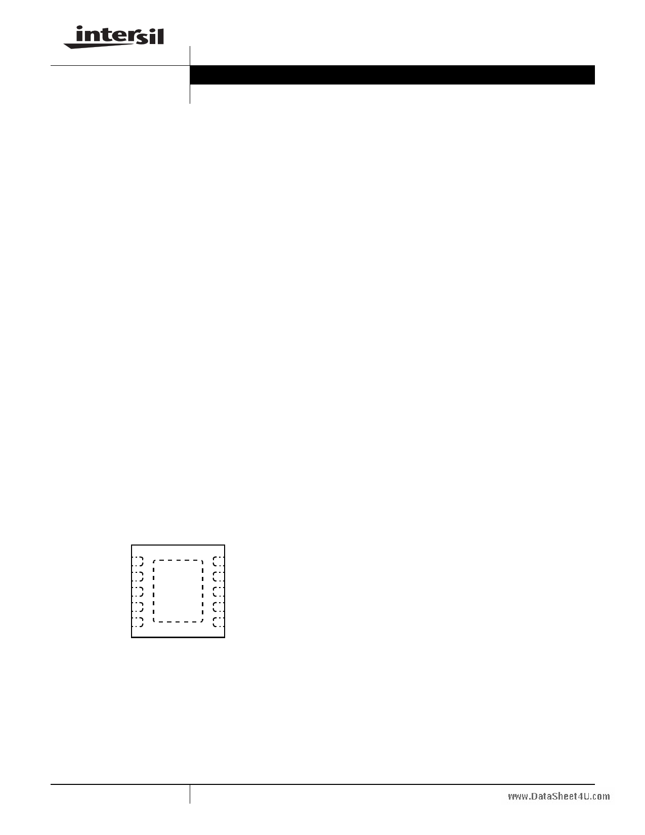
Pinout
ISL22317
(10 LD TDFN)
TOP VIEW
SCL 1
SDA 2
A1 3
REF_A 4
REF_B 5
10 VCC
9 RH
8 RW
7 RL
6 GND
Features
• Precision Digitally Controlled Potentiometer
- 99% Typical Accuracy Of Resistance Over Operational
Conditions
- Zero-Compensated Wiper Resistance
• Integrated Digitally Controlled Potentiometer
- 128-Tap Positions
- I2C Serial Interface
- Pin Selectable Slave Address
- 10kΩ, 50kΩ and 100kΩTotal Resistance
- Monotonic Over-Temperature
- Non-Volatile EEPROM Storage of Wiper Position
- 0 to VCC Terminal Voltage
• Single 2.7V to 5.5V Supply
• High Reliability
- 50 Years Retention @ ≤ +55°C
- 15 Years Retention @ +125°C
- 1,000,000 Cycles Endurance
• 3mmx3mm Thin DFN Package – 0.75mm Max Thickness,
0.65mm Pitch
• Pb-Free (RoHS Compliant)
Applications
• Setting Precise Current Values for DC Margining and
Backlight Control
• Replaces Complex Compensation Circuitry That Stores
Values in Look-up Tables Needed for Precise Resistor
Setting
• Setting Precise Resistance Values for Test and
Measurement Circuits
• Adjust Specific Resistances in Analog Circuits
• Precise Calibration and Fine Tune-Up
1 CAUTION: These devices are sensitive to electrostatic discharge; follow proper IC Handling Procedures.
I2C
Bus™
is
1-888-INTERSIL or
a trademark owned
1-888-468-3774 | Intersil (and design) and XDCP are registered trademarks of Intersil Americas Inc.
by NXP Semiconductors Netherlands, B.V. Copyright Intersil Americas Inc. 2009. All Rights Reserved
All other trademarks mentioned are the property of their respective owners.
1 page 
ISL22317
www.ODaptaeSrahetient4gU.Scopmecifications Over the recommended operating conditions unless otherwise specified. (Continued)
SYMBOL
PARAMETER
TEST CONDITIONS
MIN TYP MAX
(Note 19) (Note 4) (Note 19)
tD Power-up Delay
VRCegCisatbeor vreecVapllocro, mtopDleCtePd,InaintidalIV2CaluIneterface
in standby state
1
EEPROM SPECIFICATION
EEPROM Endurance
1,000,000
EEPROM Retention
Temperature T ≤ +55°C
50
Temperature T ≤ +125°C
15
tWC Non-volatile Write Cycle Time
(Note 18)
12 20
SERIAL INTERFACE SPECS
VIL A1, A0, SDA, and SCL Input Buffer
LOW Voltage
0.3*VCC
VIH A1, A0, SDA, and SCL Input Buffer
HIGH Voltage
0.7*VCC
Hysteresis SDA and SCL Input Buffer Hysteresis
(Note 16)
0.05*VCC
VOL SDA Output Buffer LOW Voltage,
(Note 16) Sinking 4mA
0 0.4
Cpin A1, A0, SDA, and SCL Pin
(Note 16) Capacitance
10
fSCL
tsp
SCL Frequency
Pulse Width Suppression Time at SDA Any pulse narrower than the max spec is
and SCL Inputs
suppressed
400
50
tAA
tBUF
SCL Falling Edge to SDA Output Data SCL falling edge crossing 30% of VCC, until
Valid
SDA exits the 30% to 70% of VCC window
Time the Bus must be Free Before the SDA crossing 70% of VCC during a STOP
Start of a New Transmission
condition, to SDA crossing 70% of VCC
during the following START condition
1300
900
tLOW
tHIGH
tSU:STA
Clock LOW Time
Clock HIGH Time
START Condition Setup Time
tHD:STA START Condition Hold Time
tSU:DAT Input Data Setup Time
tHD:DAT Input Data Hold Time
Measured at the 30% of VCC crossing
Measured at the 70% of VCC crossing
SCL rising edge to SDA falling edge; both
crossing 70% of VCC
From SDA falling edge crossing 30% of VCC
to SCL falling edge crossing 70% of VCC
From SDA exiting the 30% to 70% of VCC
window, to SCL rising edge crossing 30% of
VCC
From SCL rising edge crossing 70% of VCC
to SDA entering the 30% to 70% of VCC
window
1300
600
600
600
100
0
tSU:STO
tHD:STO
tDH
STOP Condition Setup Time
From SCL rising edge crossing 70% of VCC,
to SDA rising edge crossing 30% of VCC
STOP Condition Hold Time for Read, From SDA rising edge to SCL falling edge;
or Volatile Only Write
both crossing 70% of VCC
Output Data Hold Time
From SCL falling edge crossing 30% of VCC,
until SDA enters the 30% to 70% of VCC
window
600
1300
0
tR SDA and SCL Rise Time
(Note 16)
From 30% to 70% of VCC
20 +
0.1*Cb
250
UNIT
ms
Cycles
Years
Years
ms
V
V
V
V
pF
kHz
ns
ns
ns
ns
ns
ns
ns
ns
ns
ns
ns
ns
ns
5 FN6912.0
May 26, 2009
5 Page 
ISL22317
www.IDSaLta2S2h3e1e7t4. UA.cmoamximum of two ISL22317 devices may occupy
the I2C serial bus with addresses 50h and 54h.
Principles of Operation
The ISL22317 is an integrated circuit incorporating one DCP
with its associated registers, non-volatile memory and an I2C
serial interface providing direct communication between a
host and the potentiometer and memory. The resistor array
is comprised of individual resistors connected in series. At
either end of the array and between each resistor, is an
electronic switch that transfers the potential at that point to
the wiper.
The electronic switches on the device operate in a “make
before break” mode when the wiper changes tap positions.
When the device is powered down, the last value stored in
IVR will be maintained in the non-volatile memory. When
power is restored, the contents of the IVR is recalled and
loaded into the WR to set the wiper to the initial value.
DCP Description
The DCP is implemented with a combination of resistor
elements and CMOS switches. The physical ends of each
DCP are equivalent to the fixed terminals of a mechanical
potentiometer (RH and RL pins). The RW pin of the DCP is
connected to intermediate nodes, and is equivalent to the
wiper terminal of a mechanical potentiometer. The position
of the wiper terminal within the DCP is controlled by a 7-bit
volatile Wiper Register (WR). When the WR of a DCP
contains all zeroes (WR<6:0>: 00h), its wiper terminal (RW)
is closest to its “Low” terminal (RL). When the WR register of
a DCP contains all ones (WR<6:0>: 7Fh), its wiper terminal
(RW) is closest to its “High” terminal (RH). As the value of
the WR increases from all zeroes (0) to all ones (127
decimal), the wiper moves monotonically from the position
closest to RL to the closest to RH.
While the ISL22317 is being powered up, the WR is reset to
40h (64 decimal), which locates RW roughly at the center
between RL and RH. After the power supply voltage
becomes large enough for reliable non-volatile memory
reading, the WR will be reload with the value stored in a
non-volatile Initial Value Register (IVR).
The WR and IVR can be read or written to directly using the
I2C serial interface as described in the following sections.
Memory Description
The ISL22317 contains one non-volatile 8-bit Initial Value
Register (IVR), one 8-bit non-volatile Mode Select Register
(MSR), and two volatile 8-bit registers: Wiper Register (WR)
and Access Control Register (ACR). Memory map of ISL22317
is in Table 1. The non-volatile register (IVR) at address 0,
contains initial wiper position and the volatile register (WR)
contains current wiper position.
ADDRESS
(hex)
2
1
0
TABLE 1. MEMORY MAP
NON-VOLATILE
NA
Mode Select Register
IVR
VOLATILE
ACR
NA
WR
The non-volatile IVR and volatile WR registers are
accessible with the same address 0.
The ISL22317 is pre-programed with 40h in the IVR.
The Access Control Register (ACR) at address 2 contains
information and control bits described below in Table 2.
The VOL bit (ACR<7>) determines whether the access is to
wiper registers WR or initial value registers IVR.
TABLE 2. ACCESS CONTROL REGISTER (ACR)
VOL
SHDN WIP
0
0
0
0
0
(MSB)
(LSB)
If VOL bit is 0, the non-volatile IVR register is accessible. If
VOL bit is 1, only the volatile WR is accessible. Note, value
is written to IVR register also is written to the WR. The
default value of this bit is 0.
The SHDN bit (ACR<6>) disables or enables Shutdown mode.
When this bit is 0, DCP is in Shutdown mode. Default value of
SHDN bit is 1.
The WIP bit (ACR<5>) is read only bit. It indicates that
non-volatile write operation is in progress. It is impossible to
write to the WR or ACR while WIP bit is 1.
The Mode Select Bit in Mode Select Register (MSR<7>) at
address 1 allows selection of Rheostat or Voltage Divider
Mode, see Table 3.
TABLE 3. MODE SELECT REGISTER (MSR)
Mode
Select
Precision
Off
x
xxxxx
(MSB)
(LSB)
When this bit is 0, DCP is in two-terminal Rheostat Mode. In
Rheostat Mode, the RH pin should be left unconnected and
DCP can be used as variable resistor between RW and RL
pins.
When this bit is 1, DCP is in three-terminal Voltage Divider
Mode. In Voltage Divider Mode, signal is applied between
RH and RL terminals. Total resistance between RH and RL
terminals is precisely matched to external reference resistor.
Refer to reference resistor value in “Analog Specifications”
Table on page 3.
Default value of Mode Select Bit is 0.
The Precision Off bit (MSR<6>) allows the user to turn off
the matching mechanism and use the device as a regular,
11 FN6912.0
May 26, 2009
11 Page | ||
| Páginas | Total 15 Páginas | |
| PDF Descargar | [ Datasheet ISL22317.PDF ] | |
Hoja de datos destacado
| Número de pieza | Descripción | Fabricantes |
| ISL22313 | Single Digitally Controlled Potentiometer | Intersil Corporation |
| ISL22316 | Single Digitally Controlled Potentiometer | Intersil Corporation |
| ISL22316WM | Single Digitally Controlled Potentiometer | Intersil |
| ISL22317 | Precision Single Digitally Controlled Potentiometer | Intersil Corporation |
| Número de pieza | Descripción | Fabricantes |
| SLA6805M | High Voltage 3 phase Motor Driver IC. |
Sanken |
| SDC1742 | 12- and 14-Bit Hybrid Synchro / Resolver-to-Digital Converters. |
Analog Devices |
|
DataSheet.es es una pagina web que funciona como un repositorio de manuales o hoja de datos de muchos de los productos más populares, |
| DataSheet.es | 2020 | Privacy Policy | Contacto | Buscar |