|
|
PDF UP6210 Data sheet ( Hoja de datos )
| Número de pieza | UP6210 | |
| Descripción | Compact Dual Phase Synchronous Rectified Buck Controller | |
| Fabricantes | UPI Micro | |
| Logotipo |  |
|
Hay una vista previa y un enlace de descarga de UP6210 (archivo pdf) en la parte inferior de esta página. Total 16 Páginas | ||
|
No Preview Available !
www.DataSheet4U.com
Preliminary
uP6210
Compact Dual-Phase
Synchronous-Rectified Buck Controller
General Description
Features
The uP6210 is a compact dual-phase synchronous-rectified
Buck controller specifically designed to deliver high quality
output voltage for high power applications. This part is
capable of delivering up to 60A output current thanks to its
embedded bootstrapped drivers that support 12V + 12V
driving capability. The uP6210 features configurable gate
driving voltage for maximum efficiency and optimal
performance. The built-in bootstrap diode simplifies the
circuit design and reduces external part count and PCB
space.
The output voltage is precisely regulated to the reference
input that is dynamically adjustable by external voltage
divider. The uP6210 adopts DCR current sensing technique
for over current protection and droop control. The adjustable
current balance is achieved by RDS(ON) current sensing
technique.
This part features comprehensive protection functions
including over current protection, input/output under voltage
protection, over voltage protection and over temperature
protection.
Other features include adjustable soft start, adjustable
operation frequency, and quick response to step load
transient. With aforementioned functions, this part provides
customers a compact, high efficiency, well-protected and
cost-effective solutions. This part comes to VQFN4x4-24L
package.
Ordering Information
Operate with Single Supply Voltage
±2.0% Over Line Voltage and Temperature
Simple Single-Loop Voltage-Mode Control
12V Bootstrapped Drivers with Internal
Bootstrap Diode
Adjustable Over Current Protection by DCR
Current Sensing
Adjustable Current Balancing by RDS(ON) Current
Sensing
Adjustable Operation Frequency form 50kHz to
1MHz Per Phase
External Compensation
Dynamic Output Voltage Adjustment
Adjustable Soft Start
VQFN4x4-24L Package
RoHS Compliant and 100% Lead (Pb)-Free
Applications
Middle-High End GPU Core Power
High End Desktop PC Memory Core Power
Low Output Voltage, High Power Density DC-DC
Converters
Voltage Regulator Modules
Pin Configuration
Order Number Package Type
uP6210AQAG VQFN 4x4-24L
Remark
Note: uPI products are compatible with the current IPC/
JEDEC J-STD-020 and RoHS requirements. They are 100%
matte tin (Sn) plating and suitable for use in SnPb or Pb-
free soldering processes.
18 17 16 15 14 13
LG2 19
SW2 20
HG2 21
BOOT2 22
VID 23
RSET 24
GND
12 PSI
11 CSP
10 CSN
9 SS
8 EAP
7 FBRTN
123456
VQFN4x4-24L
uPI Semiconductor Corp., http://www.upi-semi.com
Rev. P00, File Name: uP6210-DS-P0000
1
1 page 
www.DataSheet4U.com
Preliminary
uP6210
Functional Description
The uP6210 is a compact dual-phase synchronous-rectified
Buck controller specifically designed to deliver high quality
output voltage for high power applications. This part is
capable of delivering up to 60A output current thanks to its
embedded bootstrapped drivers that support 12V + 12V
driving capability. The uP6210 features configurable gate
driving voltage for maximum efficiency and optimal
performance. The built-in bootstrap diode simplifies the
circuit design and reduces external part count and PCB
space.
The output voltage is precisely regulated to the reference
input that is dynamically adjustable by external voltage
divider. The uP6210 adopts DCR current sensing technique
for over current protection and droop control. The adjustable
current balance is achieved by RDS(ON) current sensing
technique.
This part features comprehensive protection functions
including over current protection, input/output under voltage
protection, over voltage protection and over temperature
protection.
Other features include adjustable soft start, adjustable
operation frequency, and quick response to step load
transient. With aforementioned functions, this part provides
customers a compact, high efficiency, well-protected and
cost-effective solutions. This part comes to VQFN4x4-24L
package.
Power On Reset and Initialization
The uP6210 works with a single supply voltage at VCC
pin. The VCC voltage is continuously monitored for power
on reset (POR) to ensure the supply voltage is high enough
for normal operation of the device. The POR threshold level
is typically 9V at VCC rising.
9V LDO for Gate Drivers
The uP6210 provides flexible gate driving voltage for
maximum efficiency and optimal performance. A linear
regulator provides 9V voltage at PVCC pin for gate drives.
9V driving voltage reduces the power dissipation at uP6210
to an acceptable level at large gate capacitance and high
switching frequency applications. Bootstrap diodes are
embedded to facilitates PCB design and reduce the total
BOM cost. No external Schottky diode is required.
Chip Enable Oscillation Frequency Programming
A resistor RRT connected to RT pin programs the oscillation
frequency as:
fOSC
=
10000
RRT (kΩ)
(kHz)
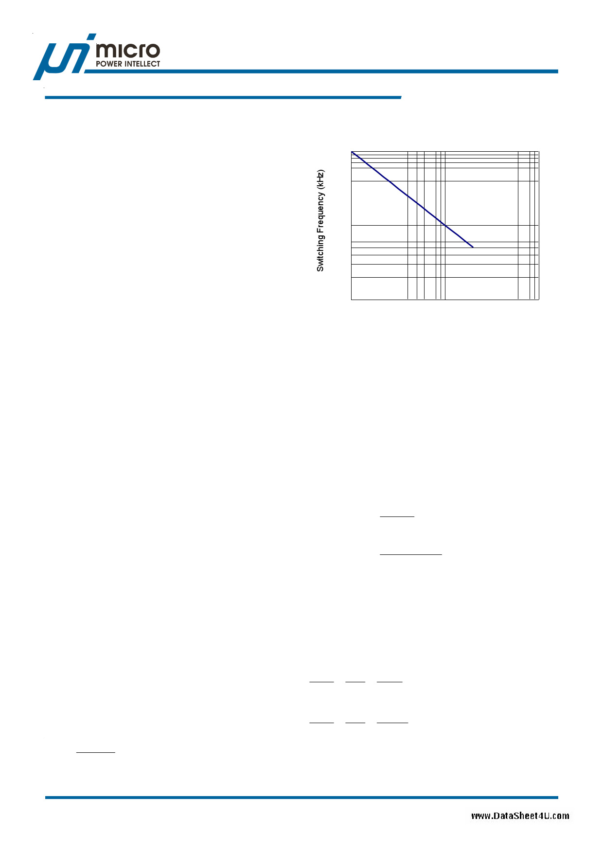
Figure 1 shows the relationship between oscillation
frequency and RRT.
1000
100
10
10 100 1000
RRT (kohm)
Figure 1. Switching Frequency vs. RRT.
When released, the RT/EN pin voltage is regulated at 1V.
Pulling the RT/EN pin to ground shuts down the uP6210.
Voltage Control Loop
Figure 2 shows the simplified voltage control loop of uP6210.
VREF is a reference voltage output with 1% accuracy and
up to 1mA sourcing capability. RSET is an open drain output
that is controlled by VID pin. RSET is pulled to FBRTN
when VID = 1 and is set high impedance when VID = 0.
Therefore, the reference input voltage at REFIN pin is
calculated as:
VREFIN
=
VREF
R2
× R1+ R2
for VID = 0
VREFIN
=
VREF
×
R2 // R3
R1+ (R2 // R3)
for VID = 1
Users can control VID pin to get two reference voltage level.
The current-limited buffer receives input at the VREFIN pin
and output a voltage source at SS pin. The output capability
of the buffer is limited to 20uA during soft start and 200uA
after soft start end. A capacitor CSS connected from SS to
FBRTN sets the voltage slew rate.
dVSS
dt
=
CSS
ISS
=
CSS
20uA
during soft start.
dVSS
dt
=
CSS
ISS
=
CSS
200uA
after soft startend.
These slew rate are used to control the output voltage slew
at soft start and VREFIN jumping respectively.
uPI Semiconductor Corp., http://www.upi-semi.com
Rev. P00, File Name: uP6210-DS-P0000
5
5 Page 
www.DataSheet4U.com
Preliminary
uP6210
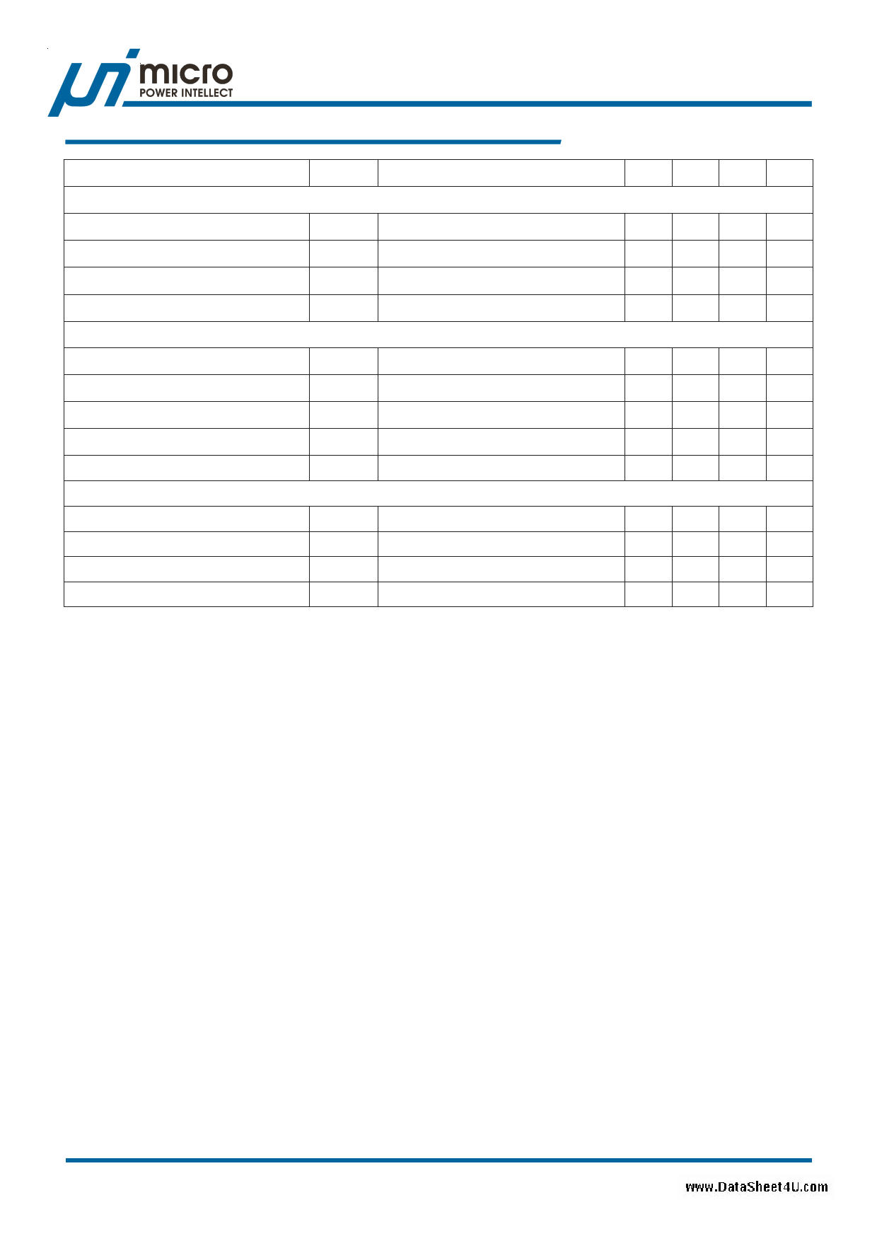
Parameter
VID Control Input
Logic High Threshold Level
Logic Low Threshold Level
On Resistrance of RSET MOSFET
Leakage of RSET Pin
Gate Driver
Upper Gate Sourcing
Upper Gate Sinking
Lower Gate Source
Lower Gate Sink
Dead Time
Protection
Over Voltage Protection
Under Voltage Protection
Over Temperature Protection
Over Temperature Hysteresis
Symbol Test Conditions
VIL
VIL
RRSET
IRSET
VID = High
VRESET = 2V, VID = 0V
RHG_SRC
RHG_SNK
RLG_SRC
RLG_SNK
TDT
IHG = 100mA sourcing
IHG = 100mA sinking
ILG = 100mA sourcing
ILG = 100mA singking
VFB - VSS
VFB - VSS
Electrical Characteristics
Min Typ Max Units
1.2 -- -- V
-- -- 0.4 V
-- 20 -- Ω
-- -- 0.1 uA
-- 2 4
-- 1.5 3
-- 2 4
-- 1 2
-- 30 --
Ω
Ω
Ω
Ω
ns
-- 300 --
-- -300 --
-- 150 --
-- 20 --
mV
mV
OC
OC
Note 1. Stresses listed as the above “Absolute Maximum Ratings” may cause permanent damage to the device.
These are for stress ratings. Functional operation of the device at these or any other conditions beyond those
indicated in the operational sections of the specifications is not implied. Exposure to absolute maximum
rating conditions for extended periods may remain possibility to affect device reliability.
Note 2. Devices are ESD sensitive. Handling precaution recommended.
Note 3. θJA is measured in the natural convection at TA = 25°C on a low effective thermal conductivity test board of
JEDEC 51-3 thermal measurement standard.
Note 4. The device is not guaranteed to function outside its operating conditions.
uPI Semiconductor Corp., http://www.upi-semi.com
Rev. P00, File Name: uP6210-DS-P0000
11
11 Page | ||
| Páginas | Total 16 Páginas | |
| PDF Descargar | [ Datasheet UP6210.PDF ] | |
Hoja de datos destacado
| Número de pieza | Descripción | Fabricantes |
| UP6210 | Compact Dual Phase Synchronous Rectified Buck Controller | UPI Micro |
| uP6213 | Multi-Phase Synchronous-Rectified Buck Controller | UPI Micro |
| Número de pieza | Descripción | Fabricantes |
| SLA6805M | High Voltage 3 phase Motor Driver IC. |
Sanken |
| SDC1742 | 12- and 14-Bit Hybrid Synchro / Resolver-to-Digital Converters. |
Analog Devices |
|
DataSheet.es es una pagina web que funciona como un repositorio de manuales o hoja de datos de muchos de los productos más populares, |
| DataSheet.es | 2020 | Privacy Policy | Contacto | Buscar |
