|
|
|
PDF ICS8344I Data sheet ( Hoja de datos )
| Número de pieza | ICS8344I | |
| Descripción | 1-TO-24 DIFFERENTIAL-TO-LVCMOS FANOUT BUFFER | |
| Fabricantes | Integrated Circuit Systems | |
| Logotipo | ||
Hay una vista previa y un enlace de descarga de ICS8344I (archivo pdf) en la parte inferior de esta página. Total 16 Páginas | ||
|
No Preview Available !
Integrated
Circuit
Systems, Inc.
ICS8344I
LOW SKEW, 1-TO-24
DIFFERENTIAL-TO-LVCMOS FANOUT BUFFER
GENERAL DESCRIPTION
The ICS8344I is a low voltage, low skew fanout
,&6 buffer and a member of the HiPerClockS™
HiPerClockS™ family of High Performance Clock Solutions from
ICS. The ICS8344I has two selectable clock in-
puts. The CLK0, nCLK0 and CLK1, nCLK1 pairs
can accept most standard differential input levels. The
ICS8344I is designed to translate any differential signal lev-
els to LVCMOS levels. The low impedance LVCMOS outputs
www.DataSheeat4rUe.dcoemsigned to drive 50Ω series or parallel terminated trans-
mission lines. The effective fanout can be increased to 48 by
utilizing the ability of the outputs to drive two series termi-
nated lines. Redundant clock applications can make use of
the dual clock input. The dual clock inputs also facilitate board
level testing. ICS8344I is characterized at full 3.3V, full 2.5V
and mixed 3.3V input and 2.5V output operating supply modes.
Guaranteed output and part-to-part skew characteristics
make the ICS8344I ideal for those clock distribution applica-
tions demanding well defined performance and repeatability.
FEATURES
• 24 LVCMOS outputs, 7Ω typical output impedance
• 2 selectable differential clock input pairs for redundant clock
applications
• CLKx, nCLKx pair can accept the following differential input
levels: LVDS, LVPECL, LVHSTL, SSTL, HCSL
• Maximum output frequency up to 100MHz
• Translates any single-ended input signal to LVCMOS with
resistor bias on nCLK input
• Multiple output enable pins for disabling unused outputs in
reduced fanout applications
• Output skew: 275ps (maximum)
• Part-to-part skew: 600ps (maximum)
• Bank skew: 150ps (maximum)
• 3.3V, 2.5V or mixed 3.3V, 2.5V operating supply modes
• -40°C to 85°C ambient operating temperature
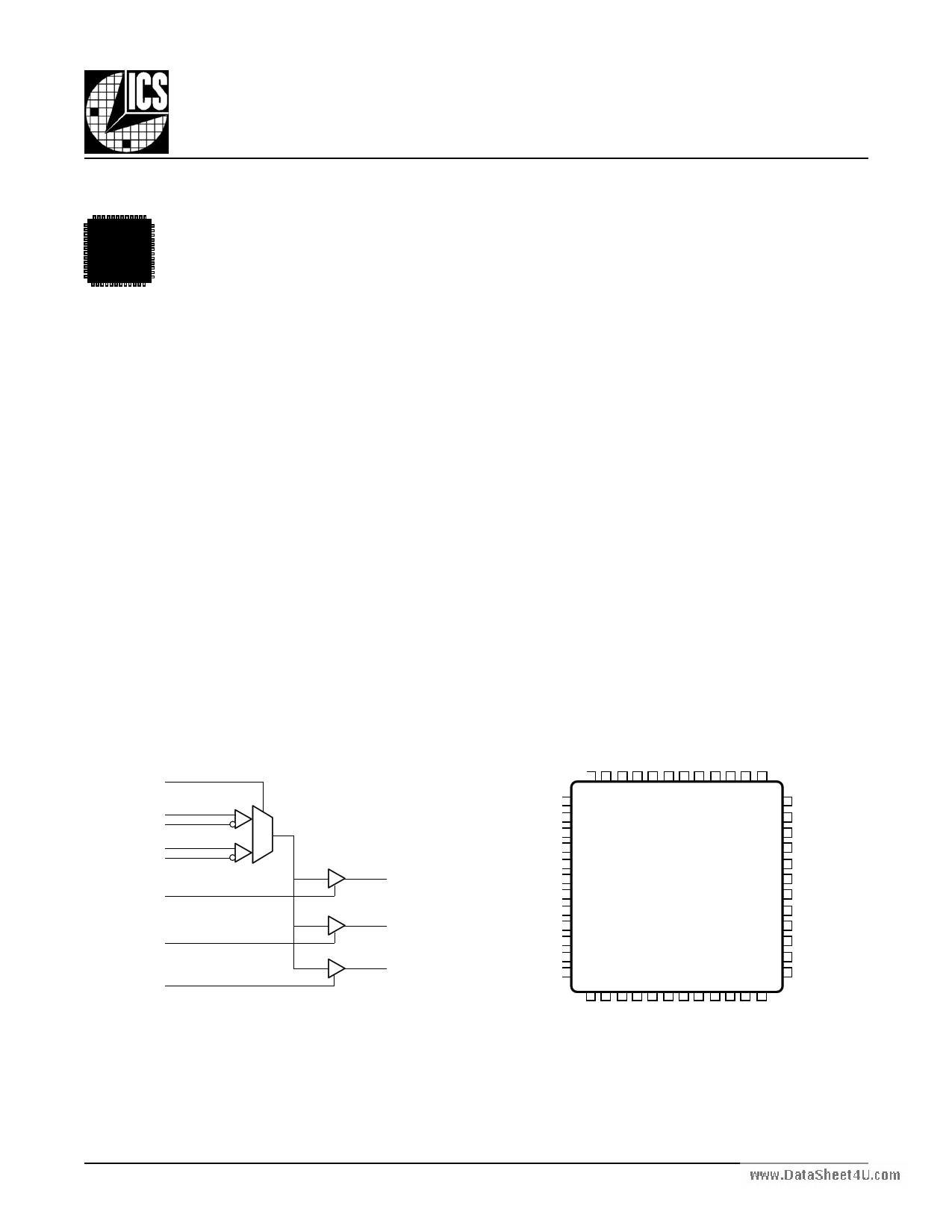
BLOCK DIAGRAM
CLK_SEL
CLK0
nCLK0
CLK1
nCLK1
OE1
OE2
OE3
0
1
8344BYI
PIN ASSIGNMENT
Q0 - Q7
Q8 - Q15
Q16 - Q23
Q16
Q17
VDDO
GND
Q18
Q19
Q20
Q21
VDDO
GND
Q22
Q23
48 47 46 45 44 43 42 41 40 39 38 37
1 36
2 35
3 34
4 33
5 32
6
7
ICS8344I
31
30
8 29
9 28
10 27
11 26
12 25
13 14 15 16 17 18 19 20 21 22 23 24
Q7
Q6
VDDO
GND
Q5
Q4
Q3
Q2
VDDO
GND
Q1
Q0
48-Lead LQFP
7mm x 7mm x 1.4mm package body
Y Package
Top View
www.icst.com/products/hiperclocks.html
1
REV. A AUGUST 9, 2001
1 page 
Integrated
Circuit
Systems, Inc.
ICS8344I
LOW SKEW, 1-TO-24
DIFFERENTIAL-TO-LVCMOS FANOUT BUFFER
TABLE 5A. AC CHARACTERISTICS, VDD = VDDO = 3.3V±5%, TA = -40°C TO 85°C
Symbol Parameter
Test Conditions
Minimum
Typical Maximum Units
fMAX Maximum Output Frequency
tpLH
Propagation Delay,
Low to High; NOTE 1
f ≤ 100MHz
2.6
100 MHz
4.3 ns
tpHL
www.DataSheett4sUk.(cbo)m
Propagation Delay,
High to Low; NOTE 1
Bank Skew; NOTE 2, 6
f ≤ 100MHz
2.4
4.3 ns
150 ps
tsk(o) Output Skew; NOTE 3, 6
275 ps
tsk(pp) Part-to-Part Skew; NOTE 4, 6
600 ps
tR Output Rise Time; NOTE 5
tF Output Fall Time; NOTE 5
odc Output Duty Cycle
30% to 70%
30% to 70%
300
300
40%
1700
1400
60%
ps
ps
%
tEN Output Enable Time; NOTE 5
f = 66.7MHz
tDIS Output Disable TIme; NOTE 5
f = 66.7MHz
All parameters measured at 100MHz unless noted otherwise.
NOTE 1: Measured from the diffferential input crossing point to VDDO/2.
NOTE 2: Defined as skew within a bank of outputs at the same voltages and with equal load conditions.
NOTE 3: Defined as skew between outputs at the same supply voltage and with equal load conditions.
Measured at VDDO/2.
NOTE 4: Defined as skew between outputs on different devices operating at the same supply voltages
and with equal load conditions. Using the same type of inputs on each device, the outputs are measured
at VDDO/2.
NOTE 5: These parameters are guaranteed by characterization. Not tested in production.
NOTE 6: This parameter is defined in accordance with JEDEC Standard 65.
5
4
ns
ns
8344BYI
www.icst.com/products/hiperclocks.html
5
REV. A AUGUST 9, 2001
5 Page 
Integrated
Circuit
Systems, Inc.
VDD
VDDO
www.DataSheet4U.com
LVCMOS
VDD = +2.05V
VDDO = +1.25V
ICS8344I
LOW SKEW, 1-TO-24
DIFFERENTIAL-TO-LVCMOS FANOUT BUFFER
SCOPE
Qx
GND = -1.25V
FIGURE 1C - 3.3V/2.5V OUTPUT LOAD TEST CIRCUIT
VDD
CLK0, CLK1
nCLK0, nCLK1
V
PP
Cross Points
V
CMR
GND
FIGURE 2 - DIFFERENTIAL INPUT LEVEL
8344BYI
Qx
Qy
t sk(o)
FIGURE 3 - OUTPUT SKEW
www.icst.com/products/hiperclocks.html
11
REV. A AUGUST 9, 2001
11 Page | ||
| Páginas | Total 16 Páginas | |
| PDF Descargar | [ Datasheet ICS8344I.PDF ] | |
Hoja de datos destacado
| Número de pieza | Descripción | Fabricantes |
| ICS8344 | 1-TO-24 DIFFERENTIAL-TO-LVCMOS FANOUT BUFFER | Integrated Circuit Systems |
| ICS8344-01 | 1-TO-24 DIFFERENTIAL-TO-LVCMOS FANOUT BUFFER | Integrated Circuit Systems |
| ICS8344I | 1-TO-24 DIFFERENTIAL-TO-LVCMOS FANOUT BUFFER | Integrated Circuit Systems |
| ICS8344I-01 | 1-TO-24 DIFFERENTIAL -TO-LVCMOS/LVTTL FANOUT BUFFER | Integrated Device Technology |
| Número de pieza | Descripción | Fabricantes |
| SLA6805M | High Voltage 3 phase Motor Driver IC. |
Sanken |
| SDC1742 | 12- and 14-Bit Hybrid Synchro / Resolver-to-Digital Converters. |
Analog Devices |
|
DataSheet.es es una pagina web que funciona como un repositorio de manuales o hoja de datos de muchos de los productos más populares, |
| DataSheet.es | 2020 | Privacy Policy | Contacto | Buscar |