|
|
|
PDF LM2931 Data sheet ( Hoja de datos )
| Número de pieza | LM2931 | |
| Descripción | LOW DROPOUT VOLTAGE REGULATORS | |
| Fabricantes | ON Semiconductor | |
| Logotipo | ||
1. LM2931 Hay una vista previa y un enlace de descarga de LM2931 (archivo pdf) en la parte inferior de esta página. Total 23 Páginas | ||
|
No Preview Available !
LM2931, NCV2931 Series
100 mA, Adjustable Output,
LDO Voltage Regulator with
60 V Load Dump Protection
The LM2931 series consists of positive fixed and adjustable output
voltage regulators that are specifically designed to maintain proper
regulation with an extremely low input−to−output voltage differential.
These devices are capable of supplying output currents in excess of
100 mA and feature a low bias current of 0.4 mA at 10 mA output.
Designed primarily to survive in the harsh automotive environment,
these devices will protect all external load circuitry from input fault
conditions caused by reverse battery connection, two battery jump
starts, and excessive line transients during load dump. This series also
includes internal current limiting, thermal shutdown, and additionally,
is able to withstand temporary power−up with mirror−image insertion.
Due to the low dropout voltage and bias current specifications, the
LM2931 series is ideally suited for battery powered industrial and
consumer equipment where an extension of useful battery life is
desirable. The ‘C’ suffix adjustable output regulators feature an output
inhibit pin which is extremely useful in microprocessor−based systems.
Features
• Input−to−Output Voltage Differential of < 0.6 V @ 100 mA
• Output Current in Excess of 100 mA
• Low Bias Current
• 60 V Load Dump Protection
• −50 V Reverse Transient Protection
• Internal Current Limiting with Thermal Shutdown
• Temporary Mirror−Image Protection
• Ideally Suited for Battery Powered Equipment
• Economical 5−Lead TO−220 Package with Two Optional Leadforms
• Available in Surface Mount SOP−8, D2PAK and DPAK Packages
• High Accuracy (±2.5%) Reference (LM2931AC) Available
• NCV Prefix for Automotive and Other Applications Requiring
Unique Site and Control Change Requirements; AEC−Q100
Qualified and PPAP Capable
• Pb−Free Packages are Available
Applications
• Battery Powered Consumer Products
• Hand−held Instruments
• Camcorders and Cameras
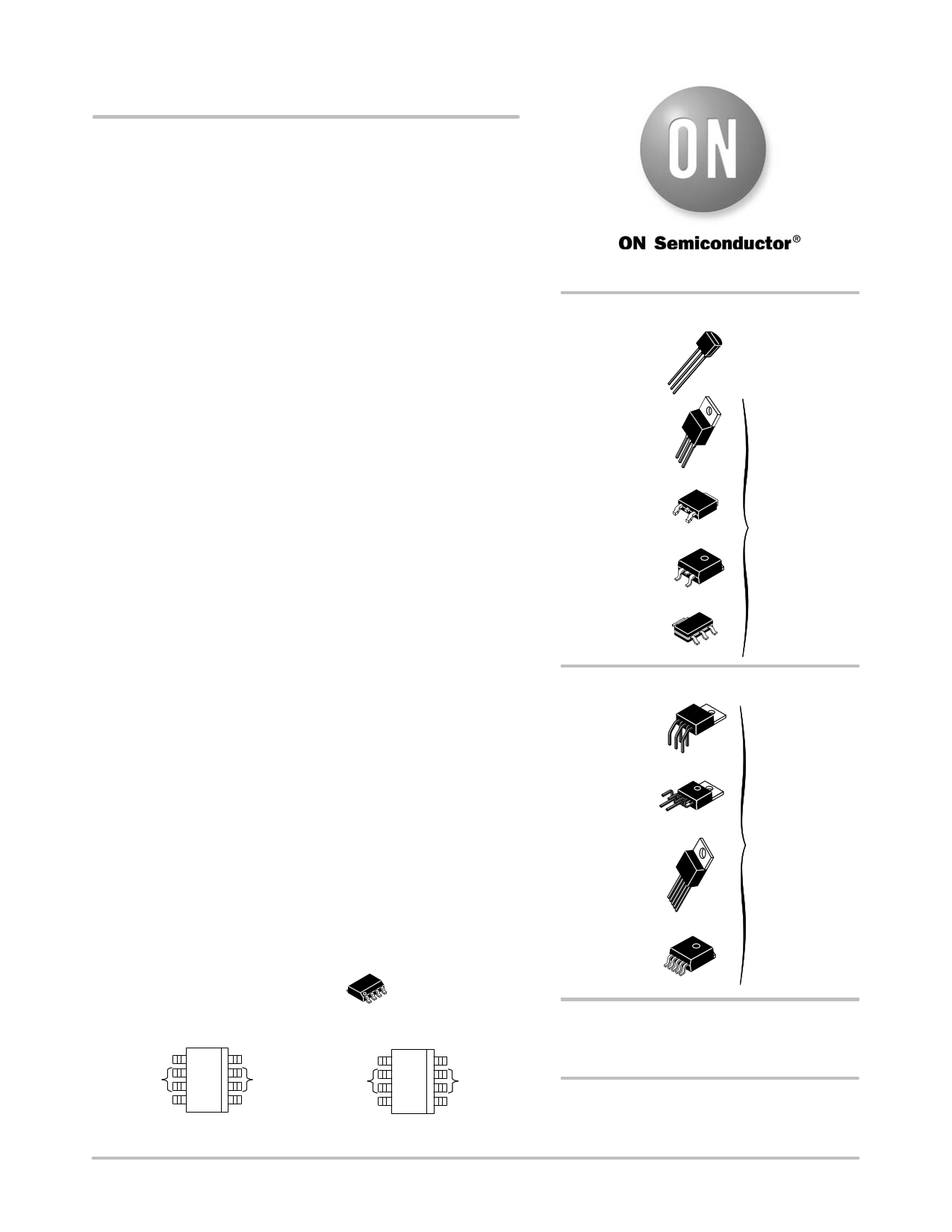
SOIC−8
D SUFFIX
CASE 751
8
1
FIXED
ADJUSTABLE
N.C. 5 4
N.C.
Output
Inhibit
54
Adjust
GND GND GND GND
Input 8 1
Output
Input 8 1
Output
(Top View)
(Top View)
http://onsemi.com
FIXED OUTPUT VOLTAGE
TO−92
Z SUFFIX
CASE 29
1
23
TO−220
T SUFFIX
CASE 221AB
1
23
DPAK
DT SUFFIX
CASE 369C
1
3
D2PAK
D2T SUFFIX
CASE 936
SOT−223
ST SUFFIX
CASE 318H
1
3
3
1
Pin 1. Output
2. Ground
3. Input
Pin 1. Input
2. Ground
3. Output
ADJUSTABLE OUTPUT VOLTAGE
TO−220
TH SUFFIX
CASE 314A
1
5
TO−220
TV SUFFIX
1
CASE 314B
5
TO−220
T SUFFIX
CASE 314D
1
Pin 1. Adjust
2. Output
Inhibit
3. Ground
4. Input
5. Output
5
D2PAK
D2T SUFFIX 1
CASE 936A
5
ORDERING INFORMATION
See detailed ordering and shipping information in the package
dimensions section on page 12 of this data sheet.
DEVICE MARKING INFORMATION
See general marking and heatsink information in the device
marking section on page 15 of this data sheet.
© Semiconductor Components Industries, LLC, 2013
April, 2013 − Rev. 26
1
Publication Order Number:
LM2931/D
1 page 
LM2931, NCV2931 Series
ELECTRICAL CHARACTERISTICS (Vin = 14 V, IO = 10 mA, CO = 100 mF, CO(ESR) = 0.3 W, TA = 25°C [Note 7])
LM2931C/NCV2931C LM2931AC/NCV2931AC
Characteristic
Symbol Min Typ Max Min Typ Max
ADJUSTABLE OUTPUT
Reference Voltage (Note 8, Figure 18)
IO = 10 mA, TA = 25°C
IO ≤ 100 mA, TA = − 40 to +125°C
Output Voltage Range
Vref
VO range
1.14
1.08
3.0 to
24
1.20
−
2.7 to
29.5
1.26
1.32
−
1.17
1.15
3.0 to
24
1.20
−
2.7 to
29.5
1.23
1.25
−
Line Regulation (Vin = VO + 0.6 V to 26 V)
Load Regulation (IO = 5.0 mA to 100 mA)
Output Impedance
IO = 10 mA, DIO = 1.0 mA, f = 10 Hz to 10 kHz
Bias Current
IO = 100 mA
IO = 10 mA
Output Inhibited (Vth(OI) = 2.5 V)
Adjustment Pin Current
Output Noise Voltage (f = 10 Hz to 100 kHz)
Long−Term Stability
Regline
−
0.2 1.5
−
0.2 1.5
Regload
−
0.3 1.0
−
0.3 1.0
ZO
− 40 −
− 40 −
IB
− 6.0 −
− 6.0 −
− 0.4 1.0 − 0.4 1.0
− 0.2 1.0 − 0.2 1.0
IAdj − 0.2 − − 0.2 −
Vn
− 140 −
− 140 −
S
− 0.4 −
− 0.4 −
Ripple Rejection (f = 120 Hz)
RR
0.10 0.003
−
0.10 0.003
−
Dropout Voltage
IO = 10 mA
IO = 100 mA
Over−Voltage Shutdown Threshold
VI−VO
Vth(OV)
− 0.015 0.2
− 0.16 0.6
26 29.5 40
− 0.015 0.2
− 0.16 0.6
26 29.5 40
Output Voltage with Reverse Polarity Input
(Vin = −15 V)
−VO −0.3 0
− −0.3 0
−
Output Inhibit Threshold Voltages
Output “On”:
Output “Off”:
TA = 25°C
TA = − 40° to +125°C
TA = 25°C
TA = − 40° to +125°C
Output Inhibit Threshold Current (Vth(OI) = 2.5 V)
Vth(OI)
Ith(OI)
−
−
2.50
3.25
−
2.15
−
2.26
−
30
1.90
1.20
−
−
50
−
−
2.50
3.25
−
2.15
−
2.26
−
30
1.90
1.20
−
−
50
7. Low duty cycle pulse techniques are used during test to maintain junction temperature as close to ambient as possible.
8. The reference voltage on the adjustable device is measured from the output to the adjust pin across R1.
Unit
V
V
mV/V
%/V
mW/V
mA
mA
mVrms/V
%/kHR
%/V
V
V
V
V
mA
http://onsemi.com
5
5 Page 
LM2931, NCV2931 Series
80 3.5
PD(max) for TA = 50°C
70 Free Air
3.0
Mounted
Vertically
60
Minimum
50 Size Pad
40
2.0 oz. Copper
L
2.5
ÎÎÎÎÎÎÎÎL 2.0
ÎÎÎÎÎÎÎÎ1.5
RqJA
30 1.0
0 5.0 10 15 20 25 30
L, LENGTH OF COPPER (mm)
Figure 26. 3−Pin and 5−Pin D2PAK
Thermal Resistance and Maximum Power
Dissipation versus P.C.B. Copper Length
300 1.8
250
PD(max) for TA = 50°C
1.6
1.4
200
2.0 oz. Copper
L
1.2
ÎÎÎ150 1.0
L 0.8
ÎÎÎÎÎÎ100 0.6
0.4
50
RqJA
0.2
0 0.0
0 5.0 10 15 20 25 30
L, LENGTH OF COPPER (mm)
Figure 27. SOT−223 Thermal Resistance and Maximum
Power Dissipation vs. P.C.B. Copper Length
DEFINITIONS
Dropout Voltage − The input/output voltage differential
at which the regulator output no longer maintains regulation
against further reductions in input voltage. Measured when
the output decreases 100 mV from nominal value at 14 V
input, dropout voltage is affected by junction temperature
and load current.
Line Regulation − The change in output voltage for a
change in the input voltage. The measurement is made under
conditions of low dissipation or by using pulse techniques
such that the average chip temperature is not significantly
affected.
Load Regulation − The change in output voltage for a
change in load current at constant chip temperature.
Maximum Power Dissipation − The maximum total
device dissipation for which the regulator will operate
within specifications.
Bias Current − That part of the input current that is not
delivered to the load.
Output Noise Voltage − The rms AC voltage at the
output, with constant load and no input ripple, measured
over a specified frequency range.
Long−Term Stability − Output voltage stability under
accelerated life test conditions with the maximum rated
voltage listed in the devices electrical characteristics and
maximum power dissipation.
http://onsemi.com
11
11 Page | ||
| Páginas | Total 23 Páginas | |
| PDF Descargar | [ Datasheet LM2931.PDF ] | |
Hoja de datos destacado
| Número de pieza | Descripción | Fabricantes |
| LM293 | Low power dual voltage comparator | NXP Semiconductors |
| LM293 | LOWPOWER DUAL VOLTAGE COMPARATORS | STMicroelectronics |
| LM293 | Low Power Low Offset Voltage Dual Comparators | National Semiconductor |
| LM293 | LMx93 LM2903 Dual Differential Comparators (Rev. Y) | Texas Instruments |
| Número de pieza | Descripción | Fabricantes |
| SLA6805M | High Voltage 3 phase Motor Driver IC. |
Sanken |
| SDC1742 | 12- and 14-Bit Hybrid Synchro / Resolver-to-Digital Converters. |
Analog Devices |
|
DataSheet.es es una pagina web que funciona como un repositorio de manuales o hoja de datos de muchos de los productos más populares, |
| DataSheet.es | 2020 | Privacy Policy | Contacto | Buscar |