|
|
|
PDF 79RC32351 Data sheet ( Hoja de datos )
| Número de pieza | 79RC32351 | |
| Descripción | IDT Interprise Integrated Communications Processor | |
| Fabricantes | Integrated Device Technology | |
| Logotipo | ||
Hay una vista previa y un enlace de descarga de 79RC32351 (archivo pdf) en la parte inferior de esta página. Total 30 Páginas | ||
|
No Preview Available !
IDTTM InterpriseTM Integrated
Communications Processor
79RC32351
Features List
◆ RC32300 32-bit Microprocessor
– Enhanced MIPS-II ISA
– Enhanced MIPS-IV cache prefetch instruction
– DSP Instructions
– MMU with 16-entry TLB
– 8kB Instruction cache, 2-way set associative
www.DataSheet4–U.c2okmB Data cache, 2-way set associative
– Per line cache locking
– Write-through and write-back cache management
– Debug interface through the EJTAG port
– Big or little endian support
◆ Interrupt Controller
– Allows status of each interrupt to be read and masked
◆ UARTs
– Two 16550 Compatible UARTs
– Baud rate support up to 1.5 Mb/s
◆ Counter/Timers
– Three general purpose 32-bit counter/timers
◆ General Purpose I/O Pins (GPIOP)
– 32 individually programmable pins:
each pin programmable as input, output, or alternate function,
input can be an interrupt or NMI source,
input can also be active high or active low
– 4 additional, auxiliary GPIO pins can be configured as input or
output
◆ SDRAM Controller
– 2 memory banks, non-interleaved, 512 MB total
– 32-bit wide data path
– Supports 4-bit, 8-bit, and 16-bit wide SDRAM chips
– SODIMM support
– Stays on page between transfers
– Automatic refresh generation
◆ Peripheral Device Controller
– 26-bit address bus
– 32-bit data bus with variable width support of 8-,16-, or 32-bits
– 8-bit boot ROM support
– 6 banks available, up to 64MB per bank
– Supports Flash ROM, PROM, SRAM, dual-port memory, and
peripheral devices
– Supports external wait-state generation, Intel or Motorola style
– Write protect capability
– Direct control of optional external data transceivers
◆ System Integrity
– Programmable system watchdog timer resets system on time-
out
– Programmable bus transaction times memory and peripheral
transactions and generates a warm reset on time-out
◆ DMA
– 14 DMA channels
– Services on-chip and external peripherals
– Supports memory-to-memory, memory-to-I/O, and I/O-to-I/O
transfers
– Supports flexible descriptor based operation and chaining via
linked lists of records (scatter / gather capability)
– Supports unaligned transfers
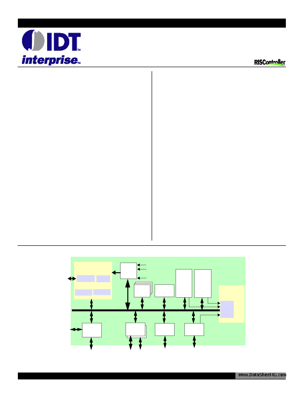
Block Diagram
RC32300
CPU Core
ICE EJTAG MMU
D. Cache I. Cache
Interrupt
Controller
:
:
3 Counter
Timers
Watchdog
Timer
10/100
Ethernet
Interface
USB
Interface
16 Channel
DMA
Controller
Arbiter
Ext. Bus
Master
SDRAM &
Device
Controller
2 UARTS
(16550)
GPIO
Interface
ATM
Interface
Memory &
Peripheral Bus
Ch. 1 Ch. 2
Serial Channels
GPIO Pins
Utopia 1 / 2
© 2002 Integrated Device Technology, Inc.
IDT and the IDT logo are trademarks of Integrated Device Technology, Inc.
1 of 42
May 25, 2004
DSC 6053
1 page 
IDT 79RC32351
Pin Description Table
The following table lists the functions of the pins provided on the RC32351. Some of the functions listed may be multiplexed onto the same pin.
To define the active polarity of a signal, a suffix will be used. Signals ending with an “N” should be interpreted as being active, or asserted, when at
a logic zero (low) level. All other signals (including clocks, buses and select lines) will be interpreted as being active, or asserted when at a logic one
(high) level.
Note: The input pads of the RC32351 do not contain internal pull-ups or pull-downs. Unused inputs should be tied off to appropriate levels.
This is especially critical for unused control signal inputs (such as BRN) which, if left floating, could adversely affect the RC32351’s opera-
tion. Also, any input pin left floating can cause a slight increase in power consumption.
Name
Type I/O Type
Description
System
www.DataSChLKeePt4U.com
COLDRSTN
I Input System Clock input. This is the system master clock input. The RISCore 32300 pipeline frequency is a multiple (x2, x3, or
x4) of this clock frequency. All other logic runs at this frequency or less.
I STI1 Cold Reset. The assertion of this signal low initiates a cold reset. This causes the RC32351 state to be initialized, boot
configuration to be loaded, and the internal processor PLL to lock onto the system clock (CLKP).
RSTN
I/O Low Drive Reset. This bidirectional signal is either driven low or tri-stated, an external pull-up is required to supply the high state. The
with STI RC32351 drives RSTN low during a reset (to inform the external system that a reset is taking place) and then tri-states it.
The external system can drive RSTN low to initiate a warm reset, and then should tri-state it.
SYSCLKP
O High Drive System clock output. This is a buffered and delayed version of the system clock input (CLKP). All SDRAM transactions
are synchronous to this clock. This pin should be externally connected to the SDRAMs and to the RC32351 SDCLKINP pin
(SDRAM clock input).
Memory and Peripheral Bus
MADDR[25:0]
O [21:0] High Memory Address Bus. 26-bit address bus for memory and peripheral accesses. MADDR[20:17] are used for the
Drive SODIMM data mask enables if SODIMM mode is selected.
MDATA[31:0]
BDIRN
BOEN[1:0]
BRN
BGN
WAITACKN
CSN[5:0]
[25:22] Low MADDR[22] Primary function: General Purpose I/O, GPIOP[27].
Drive with MADDR[23] Primary function: General Purpose I/O, GPIOP[28].
STI MADDR[24] Primary function: General Purpose I/O, GPIOP[29].
MADDR[25] Primary function: General Purpose I/O, GPIOP[30].
I/O High Drive Memory Data Bus. 32-bit data bus for memory and peripheral accesses.
O High Drive External Buffer Direction. External transceiver direction control for the memory and peripheral data bus, MDATA[31:0]. It
is asserted low during any read transaction, and remains high during write transactions.
O High Drive External Buffer Output Enable. These signals provide two output enable controls for external data bus transceivers on
the memory and peripheral data bus, MDATA. BOEN[0] is asserted low during external device read transactions. BOEN[1]
is asserted low during SDRAM read transactions.
I STI External Bus Request. This signal is asserted low by an external master device to request ownership of the memory and
peripheral bus.
O Low Drive External Bus Grant. This signal is asserted low by RC32351 to indicate that RC32351 has relinquished ownership of the
local memory and peripheral bus to an external master.
I STI Wait or Transfer Acknowledge. When configured as wait, this signal is asserted low during a memory and peripheral
device bus transaction to extend the bus cycle. When configured as transfer acknowledge, this signal is asserted low dur-
ing a memory and peripheral device bus transaction to signal the completion of the transaction.
O [3:0] Device Chip Select. These signals are used to select an external device on the memory and peripheral bus during device
High Drive transactions. Each bit is asserted low during an access to the selected external device.
CSN[4] Primary function: General purpose I/O, GPIOP[16].
[5:4] CSN[5] Primary function: General purpose I/O, GPIOP[17].
Low Drive
Table 1 Pin Descriptions (Part 1 of 7)
5 of 42
May 25, 2004
5 Page 
IDT 79RC32351
Name
Type I/O Type
Description
U0DTRN
U0DSRN
U0RTSN
U0CTSN
U0SOUTP
www.DataSheet4U.com
O Low Drive UART channel 0 data terminal ready.
Primary function: General Purpose I/O, GPIOP[4]. At reset, this pin defaults to primary function GPIOP[4] if CPU/DMA Sta-
tus Mode enable is not selected during reset using the boot configuration.
2nd Alternate function: CPU or DMA transaction indicator, CPUP.
I STI UART channel 0 data set ready.
Primary function: General Purpose I/O, GPIOP[5]. At reset, this pin defaults to primary function GPIOP[5].
O Low Drive UART channel 0 request to send.
Primary function: General Purpose I/O, GPIOP[6]. At reset, this pin defaults to primary function GPIOP[6].
I STI UART channel 0 clear to send.
Primary function: General Purpose I/O, GPIOP[7]. At reset, this pin defaults to primary function GPIOP[7].
O Low Drive UART channel 1 serial transmit.
Primary function: General Purpose I/O, GPIOP[8]. At reset, this pin defaults to primary function GPIOP[8] if DMA Debug
enable is not selected during reset using the boot configuration.
2nd Alternate function: DMA channel, DMAP[3].
U1SINP
U1DTRN
U1DSRN
I STI UART channel 1 serial receive.
Primary function: General Purpose I/O, GPIOP[9]. At reset, this pin defaults to primary function GPIOP[9] if DMA Debug
enable is not selected during reset using the boot configuration.
2nd Alternate function: DMA channel, DMAP[2].
O Low Drive UART channel 1 data terminal ready.
Primary function: General Purpose I/O, GPIOP[10]. At reset, this pin defaults to primary function GPIOP[10] if ICE Interface
enable is not selected during reset using the boot configuration.
Alternate function: PC trace status bit 0, EJTAG_PCST[0].
I STI UART channel 1 data set ready.
Primary function: General Purpose I/O, GPIOP[11]. At reset, this pin defaults to primary function GPIOP[11] if ICE Interface
enable is not selected during reset using the boot configuration.
2nd Alternate function: PC trace status bit 1, EJTAG_PCST[1].
U1RTSN
U1CTSN
O Low Drive UART channel 1 request to send.
Primary function: General Purpose I/O, GPIOP[12]. At reset, this pin defaults to primary function GPIOP[12] if ICE Interface
enable is not selected during reset using the boot configuration.
2nd Alternate function: PC trace status bit 2, EJTAG_PCST[2].
I STI UART channel 1 clear to send.
Primary function: General Purpose I/O, GPIOP[13]. At reset, this pin defaults to primary function GPIOP[13] if ICE Interface
enable is not selected during reset using the boot configuration.
2nd Alternate function: PC trace clock, EJTAG_DCLK.
1. Schmitt Trigger Input.
Table 1 Pin Descriptions (Part 7 of 7)
Boot Configuration Vector
The boot configuration vector is read into the RC32351 during cold reset. The vector defines parameters in the RC32351 that are essential to oper-
ation when cold reset is complete.
The encoding of boot configuration vector is described in Table 2, and the vector input is illustrated in Figure 6.
11 of 42
May 25, 2004
11 Page | ||
| Páginas | Total 30 Páginas | |
| PDF Descargar | [ Datasheet 79RC32351.PDF ] | |
Hoja de datos destacado
| Número de pieza | Descripción | Fabricantes |
| 79RC32351 | IDT Interprise Integrated Communications Processor | Integrated Device Technology |
| 79RC32355 | IDT Interprise Integrated Communications Processor | Integrated Device Technology |
| 79RC32355 | IDT Interprise Integrated Communications Processor | Integrated Device Technology |
| Número de pieza | Descripción | Fabricantes |
| SLA6805M | High Voltage 3 phase Motor Driver IC. |
Sanken |
| SDC1742 | 12- and 14-Bit Hybrid Synchro / Resolver-to-Digital Converters. |
Analog Devices |
|
DataSheet.es es una pagina web que funciona como un repositorio de manuales o hoja de datos de muchos de los productos más populares, |
| DataSheet.es | 2020 | Privacy Policy | Contacto | Buscar |