|
|
|
PDF TY30N50E Data sheet ( Hoja de datos )
| Número de pieza | TY30N50E | |
| Descripción | Power Field Effect Transistor | |
| Fabricantes | Motorola Semiconductors | |
| Logotipo | ||
Hay una vista previa y un enlace de descarga de TY30N50E (archivo pdf) en la parte inferior de esta página. Total 8 Páginas | ||
|
No Preview Available !
MOTOROLA
SEMICONDUCTOR TECHNICAL DATA
Designer's
™ Data Sheet
TMOS E-FET .™
Power Field Effect Transistor
N–Channel Enhancement–Mode Silicon Gate
This advanced TMOS power FET is designed to withstand high
energy in the avalanche and commutation modes. This new energy
efficient design also offers a drain–to–source diode with fast
recovery time. Designed for high voltage, high speed switching
applications in power supplies, converters, PWM motor controls,
and other inductive loads. The avalanche energy capability is
specified to eliminate the guesswork in designs where inductive
www.DataSheet4loUa.cdosmare switched and offer additional safety margin against
unexpected voltage transients.
• Avalanche Energy Specified
• Diode is Characterized for Use in Bridge Circuits
• IDSS and VDS(on) Specified at Elevated Temperature
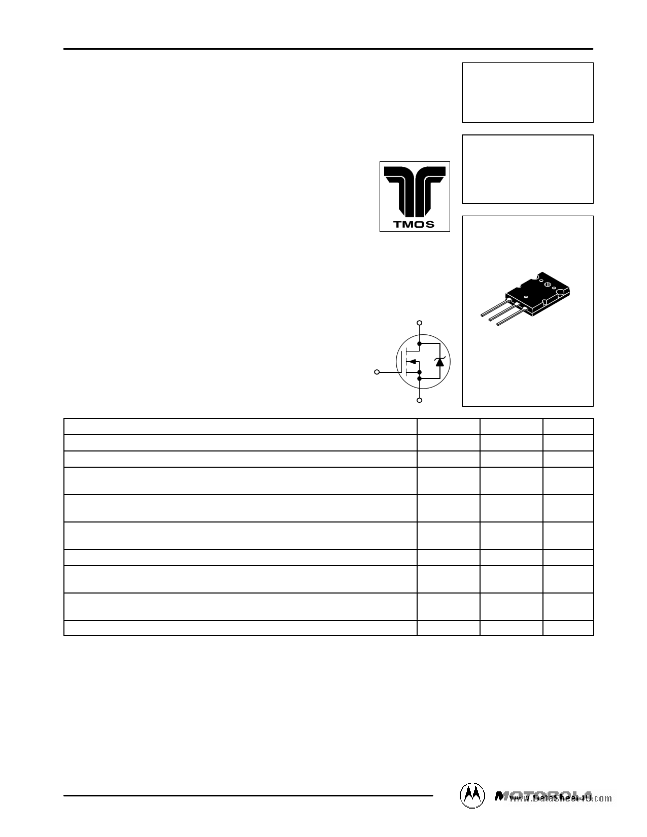
®
D
Order this document
by MTY30N50E/D
MTY30N50E
Motorola Preferred Device
TMOS POWER FET
30 AMPERES
500 VOLTS
RDS(on) = 0.15 OHM
G
MAXIMUM RATINGS (TC = 25°C unless otherwise noted)
Rating
Drain–Source Voltage
Drain–Gate Voltage (RGS = 1 MΩ)
Gate–Source Voltage — Continuous
Gate–Source Voltage — Non–Repetitive (tp ≤ 10 ms)
Drain Current — Continuous @ TC = 25°C
Drain Current — Single Pulse (tp ≤ 10 µs)
Total Power Dissipation
Derate above 25°C
Operating and Storage Temperature Range
Single Pulse Drain–to–Source Avalanche Energy — Starting TJ = 25°C
(VDD = 100 Vdc, VGS = 10 Vdc, Peak IL = 30 Apk, L = 10 mH, RG = 25 Ω )
Thermal Resistance — Junction to Case
Thermal Resistance — Junction to Ambient
Maximum Lead Temperature for Soldering Purposes, 1/8″ from case for 10 seconds
CASE 340G–02, STYLE 1
TO–264
S
Symbol
VDSS
VDGR
VGS
VGSM
ID
IDM
PD
TJ, Tstg
EAS
Value
500
500
± 20
± 40
30
80
300
2.38
– 55 to 150
3000
Unit
Vdc
Vdc
Vdc
Vpk
Adc
Apk
Watts
W/°C
°C
mJ
RθJC
RθJA
TL
0.42 °C/W
40
260 °C
Designer’s Data for “Worst Case” Conditions — The Designer’s Data Sheet permits the design of most circuits entirely from the information presented. SOA Limit
curves — representing boundaries on device characteristics — are given to facilitate “worst case” design.
E–FET and Designer’s are trademarks of Motorola, Inc.
TMOS is a registered trademark of Motorola, Inc.
Preferred devices are Motorola recommended choices for future use and best overall value.
REV 2
©MMoottoororolal,aInTc.M19O9S5 Power MOSFET Transistor Device Data
1
1 page 
12
QT
10
600
500
8 VGS 400
6
Q1
4
Q2
TJ = 25°C
ID = 30 A
2
Q3
0
0 50
VDS
100 150 200
Qg, TOTAL GATE CHARGE (nC)
300
200
100
0
250
www.DataSheet4UF.ciogmure 8. Gate Charge versus Gate–to–Source Voltage
10000
1000
VDD = 250 V
ID = 30 A
VGS = 10 V
TJ = 25°C
MTY30N50E
td(off)
100
tf
tr
td(on)
10
1 10 100
RG, GATE RESISTANCE (OHMS)
Figure 9. Resistive Switching Time
Variation versus Gate Resistance
DRAIN–TO–SOURCE DIODE CHARACTERISTICS
30
VGS = 0 V
TJ = 25°C
20
10
0
0.5 0.55 0.6 0.65 0.7 0.75 0.8 0.85 0.9 0.95
VSD, SOURCE–TO–DRAIN VOLTAGE (VOLTS)
Figure 10. Diode Forward Voltage versus Current
SAFE OPERATING AREA
The Forward Biased Safe Operating Area curves define
the maximum simultaneous drain–to–source voltage and
drain current that a transistor can handle safely when it is for-
ward biased. Curves are based upon maximum peak junc-
tion temperature and a case temperature (TC) of 25°C. Peak
repetitive pulsed power limits are determined by using the
thermal response data in conjunction with the procedures
discussed in AN569, “Transient Thermal Resistance–General
Data and Its Use.”
Switching between the off–state and the on–state may tra-
verse any load line provided neither rated peak current (IDM)
nor rated voltage (VDSS) is exceeded and the transition time
(tr,tf) do not exceed 10 µs. In addition the total power aver-
aged over a complete switching cycle must not exceed
(TJ(MAX) – TC)/(RθJC).
A Power MOSFET designated E–FET can be safely used
in switching circuits with unclamped inductive loads. For reli-
able operation, the stored energy from circuit inductance dis-
sipated in the transistor while in avalanche must be less than
the rated limit and adjusted for operating conditions differing
from those specified. Although industry practice is to rate in
terms of energy, avalanche energy capability is not a con-
stant. The energy rating decreases non–linearly with an in-
crease of peak current in avalanche and peak junction
temperature.
Although many E–FETs can withstand the stress of drain–
to–source avalanche at currents up to rated pulsed current
(IDM), the energy rating is specified at rated continuous cur-
rent (ID), in accordance with industry custom. The energy rat-
ing must be derated for temperature as shown in the
accompanying graph (Figure 12). Maximum energy at cur-
rents below rated continuous ID can safely be assumed to
equal the values indicated.
Motorola TMOS Power MOSFET Transistor Device Data
5
5 Page | ||
| Páginas | Total 8 Páginas | |
| PDF Descargar | [ Datasheet TY30N50E.PDF ] | |
Hoja de datos destacado
| Número de pieza | Descripción | Fabricantes |
| TY30N50E | Power Field Effect Transistor | Motorola Semiconductors |
| Número de pieza | Descripción | Fabricantes |
| SLA6805M | High Voltage 3 phase Motor Driver IC. |
Sanken |
| SDC1742 | 12- and 14-Bit Hybrid Synchro / Resolver-to-Digital Converters. |
Analog Devices |
|
DataSheet.es es una pagina web que funciona como un repositorio de manuales o hoja de datos de muchos de los productos más populares, |
| DataSheet.es | 2020 | Privacy Policy | Contacto | Buscar |