|
|
|
PDF DD-03182 Data sheet ( Hoja de datos )
| Número de pieza | DD-03182 | |
| Descripción | Arinc 429 Line Driver | |
| Fabricantes | DDC | |
| Logotipo | ||
Hay una vista previa y un enlace de descarga de DD-03182 (archivo pdf) en la parte inferior de esta página. Total 12 Páginas | ||
|
No Preview Available !
DD-03182 SERIES
ARINC 429 LINE DRIVER
DESCRIPTION
FEATURES
The DD-03182 device is a line driver
chip that transmits data on the serial
data bus in accordance with the
“ARINC Specification 429 Mark 33
Digital Information Transfer System”
www.DataShe(eAt4RUIN.cCom429). This device can be used
with DDC’s DD-03296 discrete-to-digi-
tal device, in conjunction with the DD-
03282 transceiver chip or the DD-
00429 microprocessor interface.
The line driver receives TTL informa-
tion on the DataA/DataB input pins
and transmits it out on the AOUT/BOUT
output pins. The output voltage level
is programmable via the VREF input
pin. The output pins are also protect-
ed against short circuits from aircraft
power. The slew rate of the DD-03182
can be programmed for either High
(100 kbit) or Low (12.5 kbit) speed via
two external timing capacitors con-
nected to the CA/CB input pins.
APPLICATIONS
The DD-03182 can be used for many
different applications ranging from
flight critical to nonessential. Surface
mount, DIP and PLCC package con-
figurations are available. Military tem-
perature range is also available if
required.
• Plastic 14-Pin SOIC Package
Available with or without Fuse
• Pin-For-Pin Alternative for Most
Harris/Holt/Raytheon Applications
• Programmable Output Voltage Level
• Short-Circuit Protection on Outputs
• Programmable Slew and Data Rates
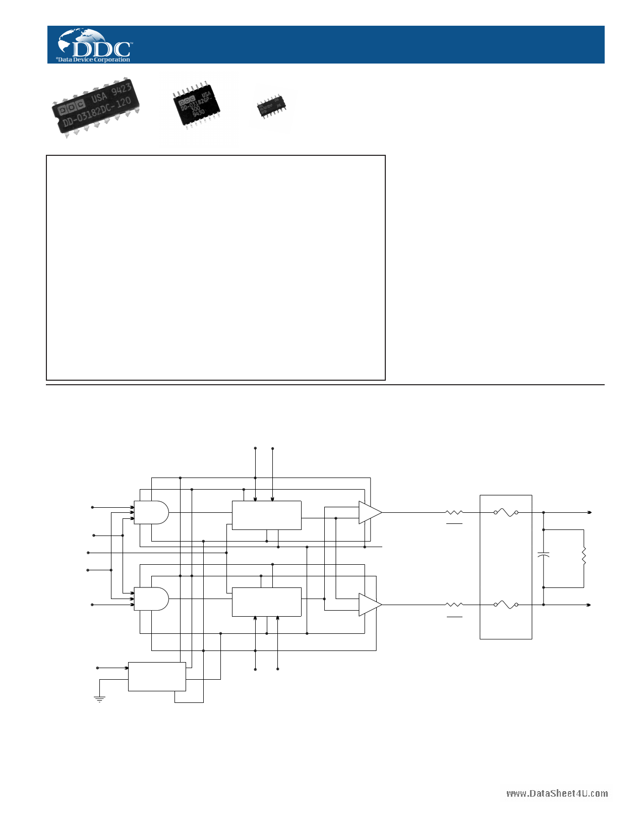
DATA (A)
CLOCK
VREF
SYNC
DATA (B)
V1 CURRENT
REGULATOR
BIAS
+V CA
LEVEL SHIFTER
AND SLOPE
CONTROL (A)
LEVEL SHIFTER
AND SLOPE
CONTROL (B)
-V CB
OUTPUT
DRIVER (A)
ROUT
2
GND
OUTPUT
DRIVER (B)
ROUT
2
OVERVOLTAGE
PROTECTION
(OPTIONAL)
AOUT
BOUT
Overvoltage Protection optional for
DD-03182VP only.
© 1993, 1999 Data Device Corporation
FIGURE 1. DD-03182 BLOCK DIAGRAM
1 page 
SLEW RATE VS. TIMING CAPACITOR VALUES
(0.4 V/µsec)(10) = 4.0 V
The output slew rates are controlled by timing capacitors CA and
CB, and are charged by ±200 µA (nominal). Slew rate (SR) is cal-
culated by:
SR = 200/C (V/µsec), where C is in pF (equation 1).
HIGH-SPEED SLEW RATE
CA and CB = 75 pF for 100 kbps
From equation 1: 200/75 = 2.67 V/µsec
10% - 90% = 0.5 V to 4.5 V
∆ = 4.0 V
For 100 kbps bit rate, the slew rate specification is 1.5 µsec
www.DataSh±e0e.t54Uµ.scoemc. Slew rate range (1.0 to 2.0 µsec).
200/SR = Capacitor, in pF
200/2.67 = 75 pF
(2.67 V/µsec)(1.5) = 4.0 V
SR = 4/(Rise Time)
4 µsec = 4V/1 µsec
Capacitor = 200/4 = 50 pF
2 µsec = 4V/2 µsec
Capacitor = 200/2 = 100 pF
LOW-SPEED SLEW RATE
CA and CB = 500 pF for 12.5 kbps
From equation 1: 200/500 = 0.4 V/µsec
For 12.5 kbps bit rate, the slew rate specification is 10 µsec
±5.0 µsec. Slew rate range (5 to 15 µsec).
200/SR = Capacitor in pF
200/0.4 = 500 pF
SR = 4/(Rise Time)
0.8 µsec = 4V/5 µsec Capacitor = 200/0.8 = 250 pF
0.267 µsec = 4V/15 µsec Capacitor = 200/0.267 = 750 pF
DD-03182 PIN FUNCTIONS
Refer to FIGURES 7, 8 and 9 and TABLE 5 for specific package
pin configurations.
VREF (Input) – the voltage on VREF sets the output voltage levels
on AOUT and BOUT. The output logic level swings between
+VREF volts, 0 volts and -VREF volts.
N/C – No Connection
SYNC (Input) – Logic 0 outputs will be forced to NULL or MARK
state. Logic 1 enables data transmission.
CLOCK (Input) – Logic 0 outputs will be forced to NULL or
MARK state. Logic 1 enables data transmission.
DATA(A)/DATA(B) (Inputs) – These signals contain the serial
data to be transmitted on the ARINC 429 data bus.
CA/CB (Analog) – External timing capacitors are tied from these
points to ground to establish the output signal slew rate.
Typically, CA=CB=75 pF for 100 kHz data and CA=CB=500 pF for
12.5 kHz data.
AOUT/BOUT (Output) – These are the line driver outputs which
are connected to the aircraft serial data bus.
-V (Input) – This is the negative supply input (-15 VDC nominal).
GND – Ground
+V (Input) – This is the positive supply input (+15 VDC nominal).
V1 (Input) – This is the logic supply input (+5 VDC nominal).
TABLE 5. DD-03182 PINOUTS
PIN NUMBER
1
DC OR GP
PACKAGE
VREF
PP PACKAGE VP PACKAGE PIN NUMBER
VREF
VREF
15
DC OR GP
PACKAGE
N/C
PP PACKAGE
GND
2
N/C N/C
N/C
16
V1
+V
3
SYNC
GND
SYNC
17
BOUT
4
DATA (A)
SYNC
DATA (A)
18
N/C
5
CA N/C
CA
19
N/C
6
AOUT
DATA (A)
AOUT
20
N/C
7
-V N/C
-V
21
N/C
8
GND
N/C
GND
22
CB
9 +V CA +V 23
DATA (B)
10 N/C N/C BOUT 24
N/C
11 BOUT N/C
CB
25
CLOCK
12
CB
N/C DATA (B)
26
N/C
13
DATA (B)
AOUT
CLOCK
27
N/C
14 CLOCK -V V1 28
V1
5
5 Page 
www.DataSheet4U.com
NOTES
11
11 Page | ||
| Páginas | Total 12 Páginas | |
| PDF Descargar | [ Datasheet DD-03182.PDF ] | |
Hoja de datos destacado
| Número de pieza | Descripción | Fabricantes |
| DD-03182 | Arinc 429 Line Driver | DDC |
| Número de pieza | Descripción | Fabricantes |
| SLA6805M | High Voltage 3 phase Motor Driver IC. |
Sanken |
| SDC1742 | 12- and 14-Bit Hybrid Synchro / Resolver-to-Digital Converters. |
Analog Devices |
|
DataSheet.es es una pagina web que funciona como un repositorio de manuales o hoja de datos de muchos de los productos más populares, |
| DataSheet.es | 2020 | Privacy Policy | Contacto | Buscar |