|
|
|
PDF PS12 Data sheet ( Hoja de datos )
| Número de pieza | PS12 | |
| Descripción | Quad Power Sequencing Controller | |
| Fabricantes | Supertex | |
| Logotipo | ||
Hay una vista previa y un enlace de descarga de PS12 (archivo pdf) en la parte inferior de esta página. Total 10 Páginas | ||
|
No Preview Available !
www.DataSheet4U.com
PS12
Quad Power Sequencing Controller
Features
► Power supply sequencer with four outputs
► Power-up and power-down sequencing
► Six programmable delays
► Maximum 90V supply voltage
► Input voltage window comparator
► Low power supply current (500µA typical)
► 16-Lead SOIC Package
Applications
► Reduction of transient current demand and
protection of sensitive loads
► Telecom and networking systems
► High voltage MEMS and display driver supplies
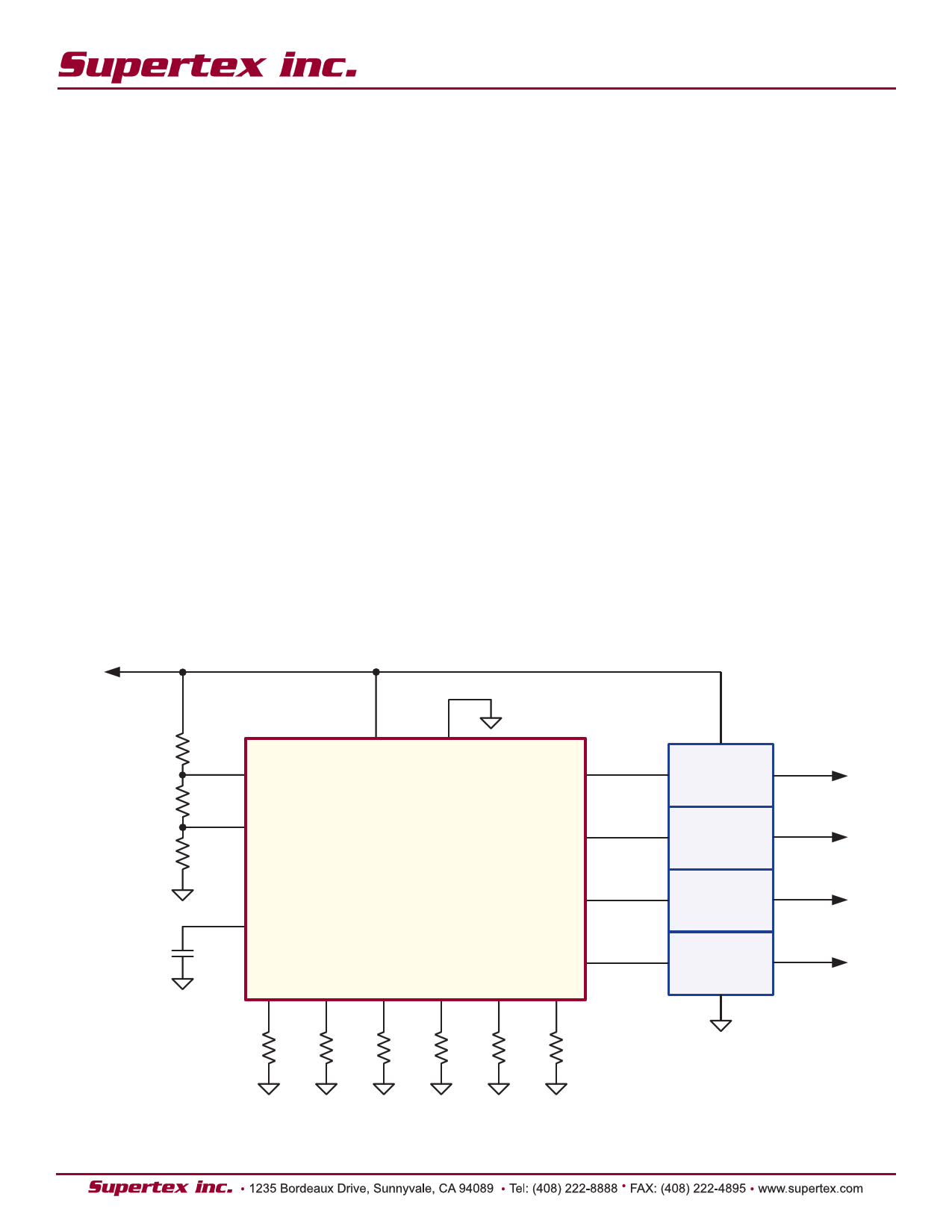
Typical Application Circuit
+12V
General Description
Many systems require that their power supplies are enabled
and disabled sequentially in order to reduce transient current
demand on the power bus, or to avoid damage to components
having multiple supply voltages such as microprocessors,
ASICs, MEMS drivers, etc.
The PS12 incorporates a power-up delay timer, a window
voltage comparator, 4 open drain enable outputs, and 6
enable delay timers. The enable delays are individually
programmable for both the power-up (ABCD) and the power-
down (DCBA) sequence.
Power-up and power-down are controlled by a window
comparator formed by the ON and OV voltage comparators.
VIN voltage within the window initiates power-up; VIN voltage
outside of the window maintains or initiates power-down. The
power-up sequence may be interrupted while in progress. The
power-down sequence, once initiated, cannot be interrupted
until it is brought to completion.
R1
3
ON
R2
4
OV
R3
2
CPUD
PUD
TAB
5
15
VIN
1
VEE
PS12NG
TBC
6
TCD
7
TDC
8
TCB
9
11
PSA
12
PSB
13
PSC
PSD
TBA
14
10
RAB
RBC
RCD
RDC
RCB
RBA
ENA
+12V
CONVERTER
ENA
+5V
CONVERTER
ENA
+3.3V
CONVERTER
ENA
+1.8V
CONVERTER
OUT
OUT
OUT
OUT
1 page 
PS12
Oscillograms
The figures of typical waveforms are organized in the following way:
Figure
Function
Description
1, 2, 3, 4
PS (A, B, C, D)
Power-up and power-down delays. Delay times around 5ms and 200ms.
5, 6 ON, PUD, PS (A, B, D) ON pin detail. Fig.6. shows a power-down / power-up sequence.
7, 8
PUD, PS (A, B)
PUD pin detail; PSA is asserted when voltage at PUD pin about 1.2V.
PUD pin resets when PSB is deasserted.
9 OV, PUD, PS (A, B) OV pin detail. Overvoltage returns to voltage window.
10
ON, PS (A, B, C)
Partial power-up sequence. Power-down triggered by loss of valid ON.
Fig.1
Fig.2
Fig.3
Fig.4
5
5 Page | ||
| Páginas | Total 10 Páginas | |
| PDF Descargar | [ Datasheet PS12.PDF ] | |
Hoja de datos destacado
| Número de pieza | Descripción | Fabricantes |
| PS10 | Quad Power Sequencing Controller | Supertex |
| PS10 | Diode ( Rectifier ) | American Microsemiconductor |
| PS1000FL | FAST RECOVERY RECTIFIERS | Compact Technology |
| PS1001 | PHOTO COUPLER INDUSTRIAL USE | NEC |
| Número de pieza | Descripción | Fabricantes |
| SLA6805M | High Voltage 3 phase Motor Driver IC. |
Sanken |
| SDC1742 | 12- and 14-Bit Hybrid Synchro / Resolver-to-Digital Converters. |
Analog Devices |
|
DataSheet.es es una pagina web que funciona como un repositorio de manuales o hoja de datos de muchos de los productos más populares, |
| DataSheet.es | 2020 | Privacy Policy | Contacto | Buscar |