|
|
|
PDF V048L015T80 Data sheet ( Hoja de datos )
| Número de pieza | V048L015T80 | |
| Descripción | Voltage Transformation Module | |
| Fabricantes | Vicor Corporation | |
| Logotipo | ||
Hay una vista previa y un enlace de descarga de V048L015T80 (archivo pdf) en la parte inferior de esta página. Total 20 Páginas | ||
|
No Preview Available !
www.DataSheet4U.com
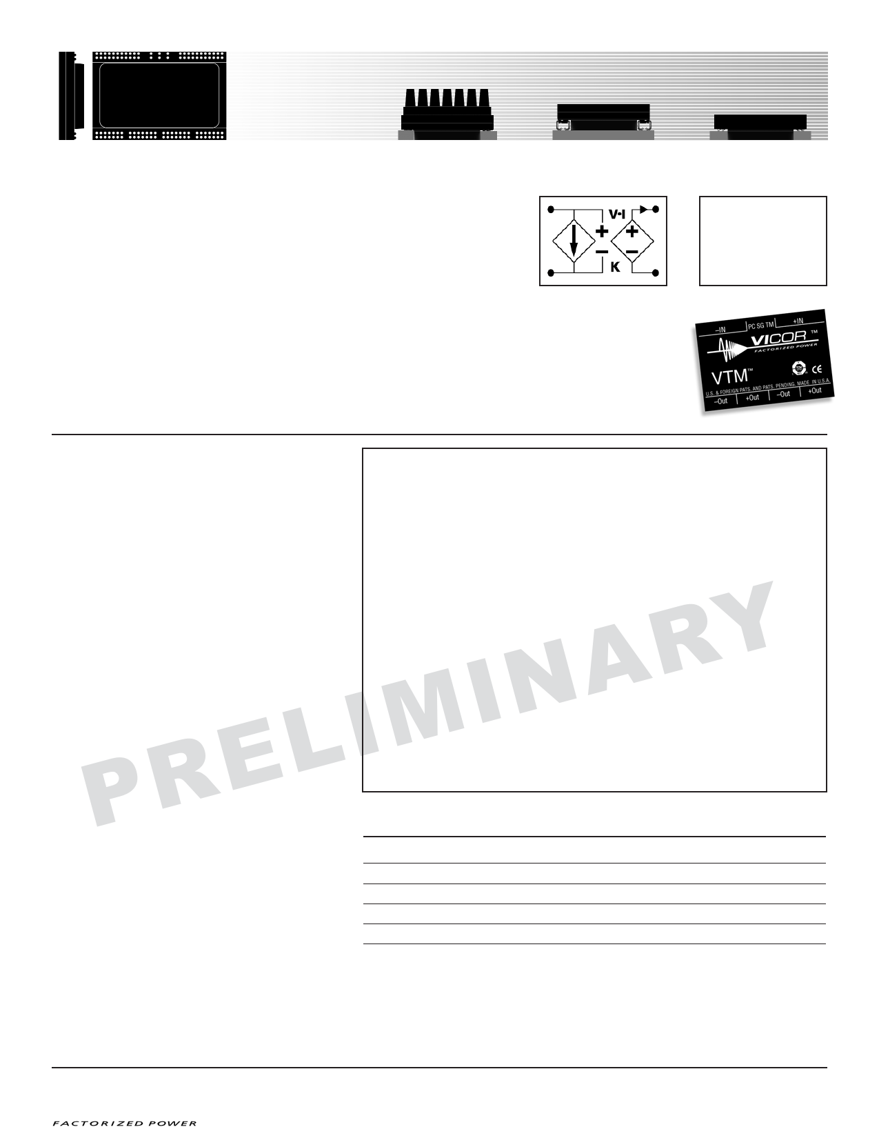
V•I ChipTM – VTM
Voltage Transformation Module
• 48V to 1.5V V•I Chip Converter
• 80 A (120 A for 1 ms)
• High density – up to 320 A/in3
• Small footprint – 80 A/in2
• Low weight – 0.4 oz (12 g)
• Pick & Place / SMD
• >92% efficiency at 1.5V
• 125°C operation
• 1 µs transient response
• >3.5 million hours MTBF
• No output filtering required
• V•I Chip BGA package
V048K015T801
Vf = 32 - 57.6 V
VOUT = 1.0 - 1.8 V
IOUT = 80 A
K = 1/32
ROUT = 1.5 mΩ max
©
Actual size
Product Description
Absolute Maximum Ratings
The V048K015T80 V•I Chip Voltage Transformation
Module (VTM) breaks records for speed, density and
Parameter
Values
Unit
Notes
efficiency to meet the demands of advanced DSP,
FPGA, ASIC, processor cores and microprocessor
applications at the point of load (POL) while providing
+In to -In
+In to -In
-1.0 to 60.0
Vdc
100 Vdc For 100 ms
isolation from input to output. It achieves a response
PC to -In
-0.3 to 7.0
Vdc
time of less than 1 µs and delivers up to 80A in a
TM to -In
-0.3 to 7.0
Vdc
volume of less than 0.25 in3 while converting 48 V to
1.5 V with unprecedented efficiency. It may be
paralleled to deliver hundreds of amps at an output
voltage settable from 1.0 to 1.8 Vdc.
P R E L I M I N A RYThe VTM V048K015T80’s nominal output voltage is
1.5 Vdc from a 48 Vdc input factorized bus, Vf, and is
controllable from 1.0 to 1.8 Vdc at no load, and from
0.9 V to 1.7 V at full load, over a Vf input range of 32 to
57.6 Vdc. It can be operated either open- or closed-loop
depending on the output regulation needs of the
application. Operating open-loop, the output voltage
tracks its Vf input voltage with a transformation ratio,
K=1/32, and an output resistance, ROUT =1.3 milliohm,
to enable applications requiring a programmable low
output voltage at high current and high efficiency.
SG to -In
+Out to -Out
Isolation voltage
Operating junction temperature
Output current
Peak output current
Case temperature during reflow
Storage temperature
Output power
Peak output power
Thermal Resistance
500
-0.5 to 5.0
1500
-40 to 125
80
120
208
-40 to 150
144
216
mA
Vdc
Vdc Input to Output
°C See note 2
A Continuous
A For 1 ms
°C
°C
W Continuous
W For 1 ms
Closing the loop back to an input Pre-Regulation
Module (PRM) or DC-DC converter may be used to
Symbol Parameter
Typ Max Units
compensate for ROUT.
RθJC
Junction-to-case
1.1 1.5 °C/W
The 1.5V VTM achieves break-through current density
of 320 A/in3 in a V•I Chip package compatible with
standard pick-and-place and surface mount assembly
processes. The V•I Chip BGA package supports in-board
mounting with a low profile of 0.16" (4mm) over the
board. A J-lead package option supports on-board
surface mounting with a profile of only 0.25" (6mm)
over the board. The VTM’s fast dynamic response and
low noise eliminate the need for bulk capacitance at the
load, substantially increasing the POL density while
improving reliability and decreasing cost.
RθJB
RθJA
RθJA
Junction-to-BGA
Junction-to-ambient 3
Junction-to-ambient 4
2.1 2.5 °C/W
6.5 7.2 °C/W
5.0 5.5 °C/W
Notes
1. For complete product matrix, see chart on page 10.
2. The referenced junction is defined as the semiconductor having the highest temperature. This
temperature is monitored by the temperature monitor (TM) signal and by a shutdown comparator.
3. V048K015T80 surface mounted in-board to a 2" x 2" FR4 board, 4 layers 2 oz Cu, 300 LFM.
4. V048L015T80 (0.25"H integral Pin Fins) surface mounted on FR4 board, 300 LFM.
45 Vicor Corporation Tel: 800-735-6200 vicorpower.com
V•I Chip Voltage Transformation Module Rev. 1.6
Page 1 of 20
1 page 
Specifications, continued
GENERAL
Parameter
Min Typ Max Unit
Note
MTBF
MIL-HDBK-217F
3.6
Mhrs
25°C, GB
Telcordia TR-NT-000332
4.2 Mhrs
Telcordia SR-332
TBD hrs
Demonstrated
TBD hrs
Isolation specifications
Voltage
1,500
Vdc Input to Output
Capacitance
5,100
6,000
pF
Input to Output
Resistance
10
MΩ Input to Output
Agency approvals (pending)
cTÜVus
UL/CSA 60950, EN 60950
CE Mark
Low voltage directive
Mechanical parameters
See mechanical drawing, Figs.16 and 18
Weight
Dimensions
Length
Width
P R E L I M I N A RYHeight
0.43 / 12.25
1.26 / 32
0.85 / 21.5
0.24 / 6
oz / g
in / mm
in / mm
in / mm
Auxiliary Pins (Conditions are at nominal line, full load, and 25°C ambient unless otherwise specified)
Parameter
Primary Control (PC)
DC voltage
Module disable voltage
Module enable voltage
Min Typ Max Unit
4.8 5.0 5.2
2.4 2.5
2.5 2.6
V
V
V
Note
Current limit
2.4 2.5 2.9 mA
Source only
Enable delay time
300 450
µs
See Fig.2
Disable delay time
4 10 µs
Temperature Monitor (TM)
27°C setting
2.95 3.00 3.05
V
Operating junction temperature
Temperature coefficient
10 mV/°C
Full range accuracy
-5 5 °C Operating junction temperature
Current limit
100
µA Source only
Figure 13— VOUT at full load vs. PC disable
Figure 14— PC signal during fault
45 Vicor Corporation Tel: 800-735-6200 vicorpower.com
V•I Chip Voltage Transformation Module Rev. 1.6
Page 5 of 20
5 Page 
Configuration Options (Cont.)
21.5
0.85
PRELIMINARY
22.0
0.87
32.0
32.0
1.26
1.26
11.7
0.46
IN–BOARD MOUNT
with 0.25'' Pin Fins
(V•I Chip recessed into PCB)
Figure 22— In-board with Pin Fins – package L
14.0
0.56
ON–BOARD MOUNT
with 0.25'' Pin Fins
mm
in
Figure 23— On-board with Pin Fins – package G
mm
in
F1
7A
Fuse
C1
100 µF
Al electrolytic
Input reflected ripple
measurement point
C2
0.47 µF
ceramic
Enable/Disable Switch
R2
2K Ω
SW1 D1
+In +Out
PC
SG VTM
TM
–In –Out
C3
100 µF
+
Load
–
Notes:
+
Temperature Monitor
–
C3 should be placed close to the load.
D1 power good indicator will dim when a module fault is detected.
TM should always be referenced to SG.
Figure 24—VTM test circuit
Application Note
Parallel Operation
In applications requiring higher current or redundancy, VTMs
can be operated in parallel without adding control circuitry or
signal lines. To maximize current sharing accuracy, it is
imperative that the source and load impedance on each VTM in
a parallel array be equal.
To achieve matched impedances, dedicated power planes
within the PC board should be used for the output and output
return paths to the array of paralleled VTMs. This technique is
preferable to using traces of varying size and length.
The VTM power train and control architecture allow bi-directional
power transfer when the VTM is operating within its specified
ranges. Bi-directional power processing improves transient
response in the event of an output load dump. The VTM may
operate in reverse, returning output power back to the input
source. It does so efficiently.
45 Vicor Corporation Tel: 800-735-6200 vicorpower.com
V•I Chip Voltage Transformation Module Rev. 1.6
Page 11 of 20
11 Page | ||
| Páginas | Total 20 Páginas | |
| PDF Descargar | [ Datasheet V048L015T80.PDF ] | |
Hoja de datos destacado
| Número de pieza | Descripción | Fabricantes |
| V048L015T80 | Voltage Transformation Module | Vicor Corporation |
| Número de pieza | Descripción | Fabricantes |
| SLA6805M | High Voltage 3 phase Motor Driver IC. |
Sanken |
| SDC1742 | 12- and 14-Bit Hybrid Synchro / Resolver-to-Digital Converters. |
Analog Devices |
|
DataSheet.es es una pagina web que funciona como un repositorio de manuales o hoja de datos de muchos de los productos más populares, |
| DataSheet.es | 2020 | Privacy Policy | Contacto | Buscar |