|
|
|
PDF 33394 Data sheet ( Hoja de datos )
| Número de pieza | 33394 | |
| Descripción | Switch Mode Power Supply | |
| Fabricantes | Freescale Semiconductor | |
| Logotipo | ||
Hay una vista previa y un enlace de descarga de 33394 (archivo pdf) en la parte inferior de esta página. Total 30 Páginas | ||
|
No Preview Available !
www.DataSheet4U.com
Freescale Semiconductor,OIrdnercth.is document from Analog Marketing
Rev. 2.5, 11/2002
Switch Mode Power Supply with
Multiple Linear Regulators and
High Speed CAN Transceiver
The 33394 is a multi–output power supply integrated circuit with high
speed CAN transceiver. The IC incorporates a switching pre–regulator
operating over a wide input voltage range from +4.0V to +26.5V (with
transients up to 45V).
The switching regulator has an internal 3.0A current limit and runs in both
buck mode or boost mode to always supply a pre–regulated output followed
by Low Drop Out (LDO) regulators: VDDH / 5.0V @ 400mA; VDD3_3 / 3.3V
@ 120mA; VDDL / 2.6V (User scalable between 3.3V – 1.25V) @ 400mA
typically, using an external NPN pass transistor. The Keep Alive regulator
VKAM (scalable) @ 50mA; FLASH memory programming voltage VPP /
5.0V or 3.3V @ 150mA; three sensor supply outputs VREF(1,2,3) / 5.0V
(tracking VDDH) @ 100mA each; and a switched battery output (VSEN) to
supply 125mA clamped to 17V.
Additional features include Active Reset circuitry watching VDDH,
VDD3_3, VDDL and VKAM, user selectable Hardware Reset Timer (HRT),
Power Sequencing circuitry guarantees the core supply voltages never
exceed their limits or polarities during system power up and power down.
A high speed CAN transceiver physical layer interfaces between the
microcontroller CMOS outputs and differential bus lines. The CAN driver is
short circuit protected and tolerant of loss of battery or ground conditions.
33394 is designed specifically to meet the needs of modules, which use
the MPC565 microcontroller, though it will also support others from the
MPC5XX family of Motorola microcontrollers.
Features:
• Wide operating input voltage range: +4.0V to +26.5V (+45V transient).
• Provides all regulated voltages for MPC5XX MCUs and other ECU’s
logic and analog functions.
• Accurate power up/down sequencing.
• Provides necessary MCU support monitoring and fail–safe support.
• Provides three 5.0 V buffer supplies for internal & external (short–circuit
protected) sensors.
• Includes step–down/step–up switching regulator to provide supply
voltages during different battery conditions.
• Interfaces Directly to Standard 5.0V I/O for CMOS Microprocessors by
means of Serial Peripheral Interface.
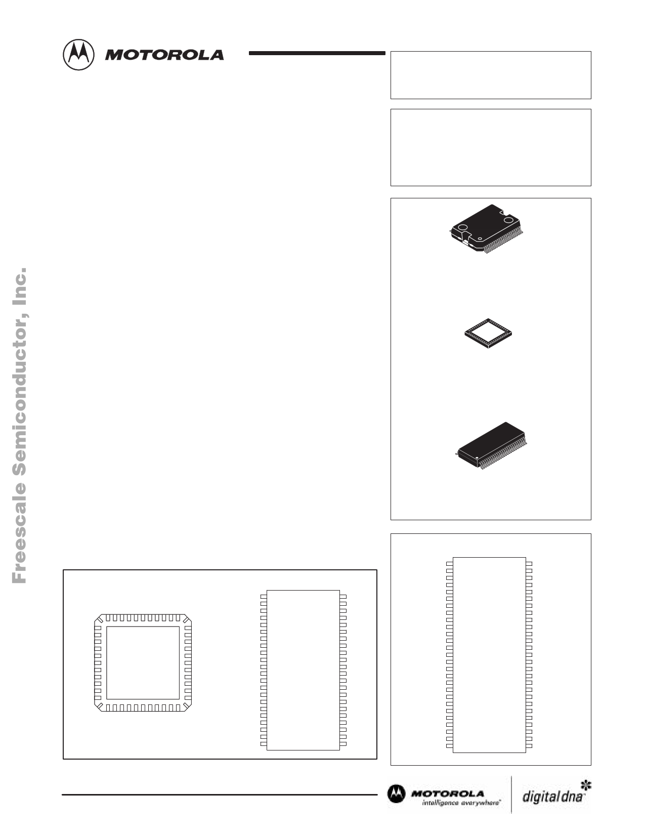
PIN CONNECTIONS
GND
SW2G
BOOT
SW1
SW1
SW1
VBAT
VBAT
KA_VBAT
VIGN
VKAM
1
QFN
TOP VIEW
VBAT
VBAT
KA_VBAT
VIGN
/SLEEP
HRT
CANH
CANL
GND
CANTXD
CANRXD
/PORESET
/HRESET
/PRERESET
VDDL_FB
VKAM
VKAM_FB
VSEN
REGON
WAKEUP
VREF1
VPP_EN
VPP
VDD3_3
VDD3_3FB
VDDL_X
VDDL_B
VDDL_FB
/PRERESET
/HRESET
/PORESET
CANRXD
CANTXD
1
HSOP
SW1
SW1
SW1
BOOT
SW2G
GND
INV
VCOMP
VPRE
VPRE_S
VDDH
VREF2
VREF3
DO
SCLK
DI
CS
/SLEEP
HRT
CANH
CANL
GND
33394
MULTI–OUTPUT
POWER SUPPLY
SEMICONDUCTOR
TECHNICAL DATA
44–Lead HSOP
DH SUFFIX
CASE 1291
44–Lead QFN
FC SUFFIX
CASE 1310
(BOTTOM VIEW)
54–Lead SOICW–EP
DWB SUFFIX
CASE 1377
PIN CONNECTIONS
GND
CANL
CANH
HRT
/SLEEP
N/C
CS
DI
SCLK
DO
N/C
VREF3
VREF2
VDDH
VPRE_S
VPRE
VCOMP
INV
GND
SW2G
BOOT
N/C
SW1
SW1
SW1
SW1
SW1
1
SOICW
CANTXD
CANRXD
/PORESET
/HRESET
/PRERESET
N/C
VDDL_FB
VDDL_B
VDDL_X
VDD3_3FB
VDD3_3
VPP
VPP_EN
VREF1
WAKEUP
REGON
VSEN
VKAM_FB
VKAM
VIGN
N/C
KA_VBAT
VBAT
VBAT
VBAT
VBAT
VBAT
This document contains information on a new product. Specifications
and information herein are subject to change without notice.
© Motorola, Inc. 2002
MOTOROLA ANALOG
For More Information On This Product,
INTEGRATED CIRCUGIToDtEoV:ICwEwDwAT.fAreescale.com
1
1 page 
Freescale Se3m33ic94onductor, Inc.
PIN FUNCTION DESCRIPTION (54 SOICW–EP Package)
PIN NO.
1
2
3
4
5
6
7
8
9
10
11
12
13
14
15
16
17
18
19
20
21
23
24
25
26
27
28
29
30
31
32
33
34
35
36
37
38
39
40
41
42
43
44
45
46
47
48
49
50
51
52
53
54
NAME
GND
CANL
CANH
HRT
/SLEEP
N/C
CS
DI
SCLK
DO
N/C
VREF3
VREF2
VDDH
VPRE_S
VPRE
VCOMP
INV
GND
SW2G
BOOT
SW1
SW1
SW1
SW1
SW1
VBAT
VBAT
VBAT
VBAT
VBAT
KA_VBAT
N/C
VIGN
VKAM
VKAM_FB
VSEN
REGON
WAKEUP
VREF1
VPP_EN
VPP
VDD3_3
VDD3_3FB
VDDL_X
VDDL_B
VDDL_FB
N/C
/PRERESET
/HRESET
/PORESET
CANRXD
CANTXD
DESCRIPTION
Ground
CAN differential bus drive low line
CAN differential bus drive high line
Hardware Reset Timer pin (programmed with external capacitor and resistor)
Sleep Mode & Power Down control
No Connect
SPI chip select
SPI serial data in
SPI clock input
SPI serial data out
No Connect
VDDH tracking linear regulator 3
VDDH tracking linear regulator 2
5.0 V regulated supply output
Switching pre–regulator output sense
Switching pre–regulator output
Switching pre–regulator compensation (error amplifier output)
Switching pre–regulator error amplifier inverting input
Ground
External power switch (MOSFET) gate drive — Boost regulator
Bootstrap capacitor
Source of the internal power switch (n–channel MOSFET)
Source of the internal power switch (n–channel MOSFET)
Source of the internal power switch (n–channel MOSFET)
Source of the internal power switch (n–channel MOSFET)
Source of the internal power switch (n–channel MOSFET)
Battery supply to IC (external reverse battery protection needed in some applications)
Battery supply to IC (external reverse battery protection needed in some applications)
Battery supply to IC (external reverse battery protection needed in some applications)
Battery supply to IC (external reverse battery protection needed in some applications)
Battery supply to IC (external reverse battery protection needed in some applications)
Keep alive supply (with internal protection diode)
No Connect
Turn–On control through ignition switch (with internal protection diode)
VDDL tracking Keep Alive Memory (Standby) supply
VKAM output feedback
Switched battery output
Regulator “Hold On” input
CAN wake up event output
VDDH tracking linear regulator 1
VPP enable
5.0 V/ 3.3 V FLASH memory programming supply, tracking VDDH/VDD3_3
3.3 V regulated supply output, base drive for optional external pass transistor
VDD3_3 output feedback
VDDL optional external pass transistor base drive, operating in Boost Mode only
VDDL external pass transistor base drive
VDDL output feedback
No Connect
Open drain /PRERESET output, occurs 0.7 us prior to /HRESET (Hardware Reset)
Open drain / HRESET (Hardware Reset) output
Open drain / PORESET (Power On Reset) supervising VKAM supply to the microprocessor.
CAN receive data (DOUT)
CAN transmit data (DIN)
NOTE: The exposed pad of the 54 SOICW–EP package is electrically and thermally connected with the IC ground.
For More Information On This Product,
MOTOROLA ANALOG INTEGRATED CIRCUGIToDtEoV:ICwEwDwAT.fAreescale.com
5
5 Page 
Freescale Se3m33ic94onductor, Inc.
3. ELECTRICAL CHARACTERISTICS (–40°C ≤ TA ≤ +125°C; +4.0 V ≤ VBAT ≤ +26.5 V using the 33394 typical application
circuit – see Figure 1, unless otherwise noted.)
Characteristic
Symbol
Min.
Typ.
Max.
Unit
DC CHARACTERISTICS:
VREF1, 2, 3
VREF Output Voltage, IVREF = –100 mA
VREF
4.86 5.0 5.12 V
VREF Load Regulation, VBAT = 13.3 V; IVREF = 0 to –100 mA
LoadRgVREF
–40
40 mV
VREF Line Regulation, VBAT = 4.0 V to 26.5 V; IVREF = –100 mA
LineRgVREF
–20
20 mV
VREF Tracking to VDDH Voltage, VDDH – VREF,
VBAT = 4.0 V to 26.5 V, IVREF = 0 to –100 mA;
IVDDH = 0 to –400 mA
VTVREF
–40
20 mV
VREF Drop Out Voltage, VPRE–VREF
IVREF = –100 mA; Decrease VBAT until VREF is out of specification
(less than 4.86 V)
VDOV
0.4 V
VREF Output Current, VBAT = 4.0 V to 26.5 V
VREF Short Circuit Current, VREF = –2.0 V
VREF Short to Battery Load Current, VBAT = 18 V, VREF = 18 V
VREF Leakage Current, VREF disabled, VREF = –2.0 V
Thermal Shutdown Junction Temperature
(Note 1)
Thermal Shutdown Hysteresis
(Note 1)
VSEN
VSEN Saturation Voltage, IVSEN = 0 to –125 mA, VBAT= 8 to 16 V
VSEN Output Voltage Limit, IVSEN = 0 to –125mA, VBAT= 16 to 26.5V
VSEN Short Circuit Current, VSEN = –2.0 V
VSEN Short to Battery Load Current, VBAT = 18 V, VSEN = 18 V
VSEN Leakage Current, VSEN disabled, VSEN = –2.0 V
Thermal Shutdown Junction Temperature
(Note 1)
Thermal Shutdown Hysteresis
(Note 1)
NOTE:
1. Guaranteed by design but not production tested.
IVREF
ISC
IstbVREF
ILKVREF
TSDIS
TSHYS
VSENsat
VSENlimit
IscVSEN
IstbVSEN
ILKVSEN
TSDIS
TSHYS
–260
–2.0
150
5.0
16
–290
150
5.0
–100
17
–110
40
190
20
0.2
21
–140
40
200
190
20
mA
mA
mA
mA
°C
°C
V
V
mA
mA
µA
°C
°C
For More Information On This Product,
MOTOROLA ANALOG INTEGRATED CIRCUGIToDtEoV:ICwEwDwAT.fAreescale.com
11
11 Page | ||
| Páginas | Total 30 Páginas | |
| PDF Descargar | [ Datasheet 33394.PDF ] | |
Hoja de datos destacado
| Número de pieza | Descripción | Fabricantes |
| 33390 | Class B Serial Transceiver | Motorola Inc |
| 33394 | Switch Mode Power Supply | Freescale Semiconductor |
| 33395 | Three-Phase Gate Driver IC | Freescale Semiconductor |
| 33395T | Three-Phase Gate Driver IC | Freescale Semiconductor |
| Número de pieza | Descripción | Fabricantes |
| SLA6805M | High Voltage 3 phase Motor Driver IC. |
Sanken |
| SDC1742 | 12- and 14-Bit Hybrid Synchro / Resolver-to-Digital Converters. |
Analog Devices |
|
DataSheet.es es una pagina web que funciona como un repositorio de manuales o hoja de datos de muchos de los productos más populares, |
| DataSheet.es | 2020 | Privacy Policy | Contacto | Buscar |