|
|
PDF 33291 Data sheet ( Hoja de datos )
| Número de pieza | 33291 | |
| Descripción | Eight-Output Switch | |
| Fabricantes | Freescale Semiconductor | |
| Logotipo | ||
Hay una vista previa y un enlace de descarga de 33291 (archivo pdf) en la parte inferior de esta página. Total 26 Páginas | ||
|
No Preview Available !
www.DFaretaeSshceeatl4eUS.ceommiconductor
Technical Data
Eight-Output Switch with Serial
Peripheral Interface I/O
Document Number: MC33291
Rev. 4.0, 10/2006
33291
The 33291 device is an eight-output, low-side power switch with 8-
bit serial input control. The 33291 is a versatile circuit designed for
automotive applications, but is well suited for other environments. The
33291 incorporates SMARTMOS technology, with CMOS logic,
bipolar/MOS analog circuitry, and DMOS power MOSFETs. The 33291
interfaces directly with a microcontroller to control various inductive or
incandescent loads.
The circuit’s innovative monitoring and protection features include
very low standby current, SPI cascade fault reporting capability,
internal 53 V clamp on each output, output-specific diagnostics, and
independent shutdown of outputs.
The device is parametrically specified over an ambient temperature
range of -40°C ≤ TA ≤ 125°C and 9.0 V ≤ VPWR ≤ 16 V supply.
Features
• Designed to Operate Over Wide Supply Voltages of 5.5 V to 26.5 V
• Interfaces to Microprocessor Using 8-Bit SPI I/O Protocol up to 3.0
MHz
• 1.0 A Peak Current Outputs with Maximum RDS(ON) of 1.6 Ω at TJ -
150°C
• Outputs Current-Limited to Accommodate In-Rush Currents
Associated with Switching Incandescent Loads
• Output Voltages Clamped to 53 V During Inductive Switching
• Maximum Sleep Current (IPWR) of 25 µA
• Maximum of 4.0 mA IDD During Operation
• Pb-Free Packaging Designated by Suffix Code EG
LOW-SIDE SWITCH
DW SUFFIX
EG SUFFIX (PB-FREE)
98ASB42344B
24-PIN SOICW
ORDERING INFORMATION
Device
Temperature
Range (TA)
Package
MC33291DW/R2
MCZ33291EG/R2
-40°C to 125°C
24 SOICW
VDD
MCU
33291
VPWR OP 0
SFPD OP 1
VDD OP 2
CS
SCLK
SI
SO
RESET
OP 3
OP 4
OP 5
OP 6
OP 7
GND
V PWR
Figure 1. 33291 Simplified Application Schematic
Freescale Semiconductor, Inc. reserves the right to change the detail specifications, as
may be required, to permit improvements in the design of its products.
© Freescale Semiconductor, Inc., 2006. All rights reserved.
1 page 
ELECTRICAL CHARACTERISTICS
MAXIMUM RATINGS
Table 3. Maximum Ratings (continued)
All voltages are with respect to ground unless otherwise noted. Exceeding these ratings may cause a malfunction or
permanent damage to the device.
Rating
Symbol
Value
Unit
Thermal Resistance
Junction-to-Ambient (Natural Convection, Single-Layer Board) (12), (13)
Junction-to-Ambient (Natural Convection, Four-Layer Board) (12), (14)
Junction to Board (15)
RθJA
RθJMA
RθJL
°C/W
68
44
20
Notes
12. Junction temperature is a function of die size, on-chip power dissipation, package thermal resistance, mounting site (board)
temperature, ambient temperature, air flow, power dissipation of other components on the board, and board thermal resistance.
13. Per SEMI G38-87 and JEDEC JESD51-2 with the single layer board (JESD51-3) horizontal.
14. Per JEDEC JESD51-6 with the board (JESD51-7) horizontal.
15. Thermal resistance between the die and the printed circuit board per JEDEC JESD51-8.
Analog Integrated Circuit Device Data
Freescale Semiconductor
33291
5
5 Page 
ELECTRICAL CHARACTERISTICS
ELECTRICAL PERFORMANCE CURVES
tR(SI)
< 50 ns
tF(SI)
< 50 ns
90%
50%
CS 10%
tDLY(OFF)
Output Voltage
Waveform 1
10%
5.0 V
0
14 V
VOL
Output Voltage
Waveform 2
90%
tDLY(ON)
14 V
VOL
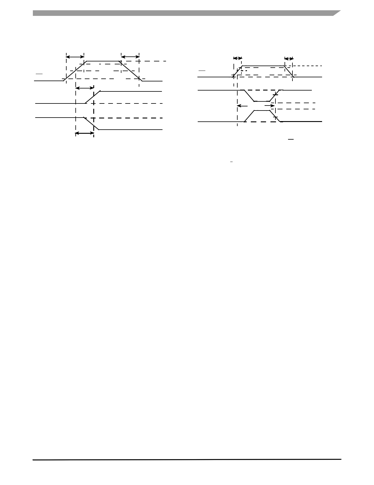
1. tDLY(ON) and tDLY(OFF) are turn-ON and turn-OFF propagation delay
times.
2. Turn-OFF is an output programmed from an ON to an OFF state.
3. Turn-ON is an output programmed from and OFF to an ON state.
Figure 11. Turn-On/-Off Waveforms
tR(SI)
tF(SI)
< 50 ns
< 50 ns
50% 90%
CS 10%
5.0 V
0
Output Voltage
Waveform
Output Current
Waveform
50%
tPDLY(OFF)
50%
VOFF = 11 V
VON = 5.0 V
IO(CL)
0
1. tPDLY(OFF) is the output fault unlatch disable propagation delay time re-
quired to correctly report an output fault after CS rises. It represents an
output commanded ON while having an existing output short (overcurrent)
to supply.
2. The SFPD pin < 0.2 V.
Figure 12. Output Fault Unlatch Disable
Delay Waveforms
Analog Integrated Circuit Device Data
Freescale Semiconductor
33291
11
11 Page | ||
| Páginas | Total 26 Páginas | |
| PDF Descargar | [ Datasheet 33291.PDF ] | |
Hoja de datos destacado
| Número de pieza | Descripción | Fabricantes |
| 3329 | 66-channel GPS Engine Board Antenna Module | Mediatek_3329 |
| 33291 | Eight-Output Switch | Freescale Semiconductor |
| 33291L | Eight-Output Switch | Freescale Semiconductor |
| 3329H | Circularity/ Single Turn /Trimming Potentiometer | DB Lectro |
| Número de pieza | Descripción | Fabricantes |
| SLA6805M | High Voltage 3 phase Motor Driver IC. |
Sanken |
| SDC1742 | 12- and 14-Bit Hybrid Synchro / Resolver-to-Digital Converters. |
Analog Devices |
|
DataSheet.es es una pagina web que funciona como un repositorio de manuales o hoja de datos de muchos de los productos más populares, |
| DataSheet.es | 2020 | Privacy Policy | Contacto | Buscar |
