|
|
|
PDF 33099 Data sheet ( Hoja de datos )
| Número de pieza | 33099 | |
| Descripción | Adaptive Alternator Voltage Regulator | |
| Fabricantes | Freescale Semiconductor | |
| Logotipo | ||
Hay una vista previa y un enlace de descarga de 33099 (archivo pdf) en la parte inferior de esta página. Total 18 Páginas | ||
|
No Preview Available !
www.DFarteaeSshceeatl4eUS.ceommiconductor
Technical Data
Adaptive Alternator Voltage
Regulator
The 33099 is designed to regulate the output voltage in diode-
rectified alternator charging systems common to automotive
applications. The 33099 provides either an analog or digital fixed
frequency duty cycle (ON/OFF ratio) control of an alternator’s field
current. Load Response Control (LRC) of the alternator field current
is accomplished by selecting the duty cycle for prevailing engine
conditions to eliminate engine speed hunting and vibrations caused
by abrupt torque loading of the engine owing to sudden electrical
loads being applied to the system at low engine RPM. Four LRC rates
are selectable by connecting pins 7 and 8 to ground.
The 33099 uses a feedback voltage to establish an alternator field
current that is in harmony with system load currents. The output
voltage is monitored by an internal voltage divider scheme and
compared to an internal voltage ramp referenced to a bandgap
voltage. This approach provides precision output voltage control over
a wide range of temperature, electrical loads, and engine RPM.
Features
• External High-Side MOSFET Control of a Ground-Referenced
Field Winding
• LRC Active During Initial Start
• Vset at ±0.1 V @ 25°C
• <0.1 V Variation Over Engine Speeds of 2,000 to 10,000 RPM
• <0.2 V Variation Over 10% to 95% of Maximum Field Current
• Controlled MOSFET and Field Flyback Diode Recovery
Characteristics for Minimum RFI
• Trimmed Devices Available at 14.6 V and 14.8 V (typical) Vset
• Pb-Free Packaging Designated by Suffix Code EG
Document Number: MC33099
Rev. 6.0, 1/2007
33099
VOLTAGE REGULATOR
DW SUFFIX
EG SUFFIX (PB-FREE)
98ASB42567B
16-PIN SOICW
ORDERING INFORMATION
Device
Temperature
Range (TA)
Package
MC33099DW/R2
MC33099CDW/R2
MCZ33099EG/R2
MCZ33099CEG/R2
-40°C to 125°C
16 SOICW
16 SOICW
(Pb-FREE)
33099
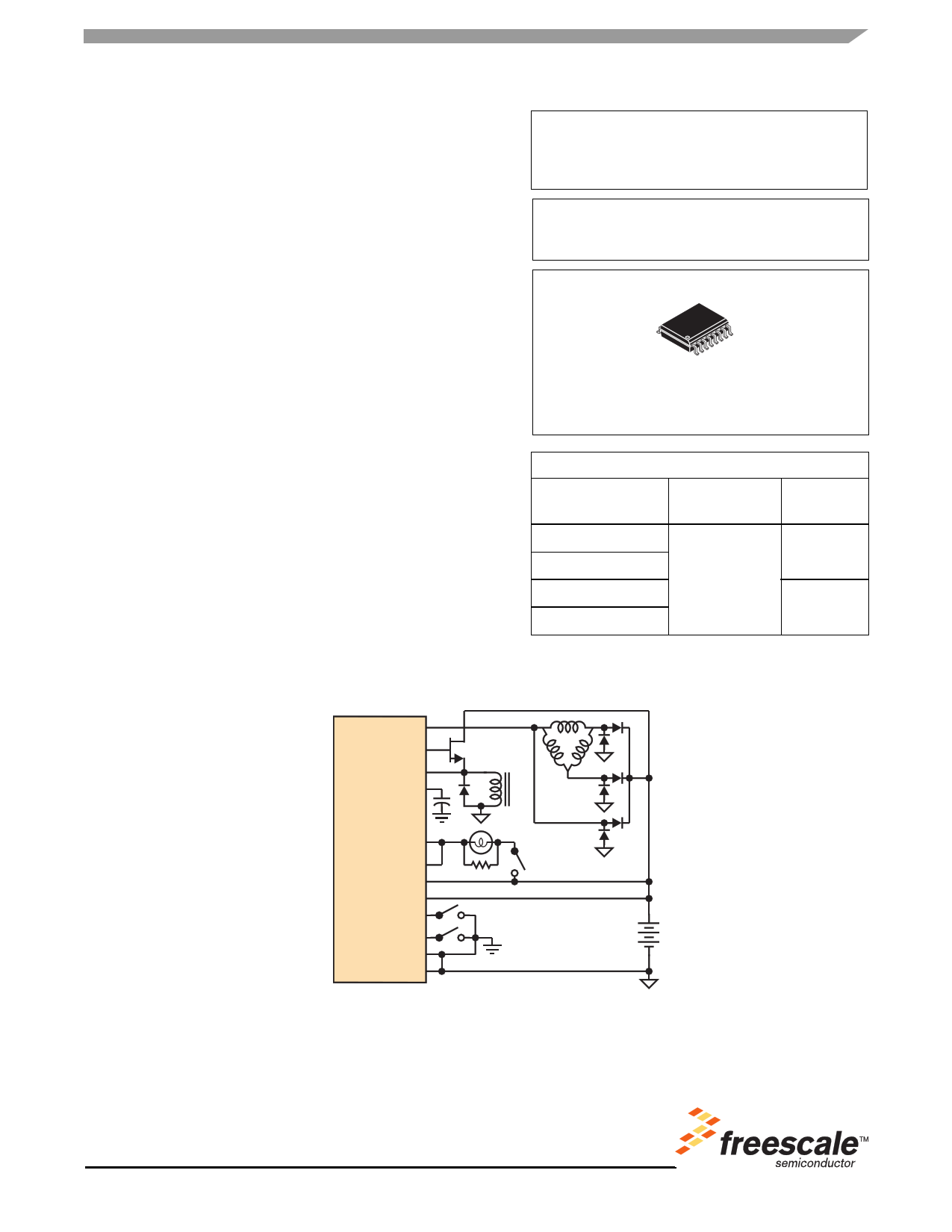
PHASE
GATE
SOURCE
PHASE FILTER
FIELD
WINDING
IGN
LAMP DRAIN
BAT
REMOTE
LRC1
LRC2
AGND
GND
IGNITION
SWITCH
CHASSIS
Figure 1. 33099 Simplified Application Diagram
© Freescale Semiconductor, Inc., 2007. All rights reserved.
1 page 
ELECTRICAL CHARACTERISTICS
STATIC ELECTRICAL CHARACTERISTICS
STATIC ELECTRICAL CHARACTERISTICS
Table 3. Static Electrical Characteristics
Characteristics noted under conditions 7.0 V ≤ VSUP ≤ 18 V, -40°C ≤ TA ≤ 125°C, GND = 0 V unless otherwise noted. Typical
values noted reflect the approximate parameter means at TA = 25°C under nominal conditions unless otherwise noted.
Characteristic
Symbol Min Typ Max Unit
Regulation Voltage @ 50% Duty Cycle
Vrem = Vset or Vrem < VTrem MC33099
Vrem = Vset or Vrem < VTrem MC33099C
VSET
14.55
14.3
14.8
14.6
15.05
14.85
V
Regulation Voltage Range
10% < DC < 95%
Regulation Voltage Temperature Coefficient (TC)
Vrem = Vbat or Vrem < VTrem
DVSET
mV
– 210 300
TC (VSET)
-13
-11
mV/°C
-9
Power Up/Down IGN Threshold Voltage
Operating Drain Current (Ignition ON)
Vign > VTign, Vrem = Vph = Vset, TA = 25°C
Vign > VTign, Vrem = Vph = Vset, -40°C ≤ TA ≤ 125°C
VTIGN
0.9 1.25 1.6 V
mA
IQ1(ON) – 6.5 8.0
IQ2(ON) – 6.5 8.4
Standby Drain Current (Ignition OFF)
Vign < VTign, Vph = 0 V, Vrem = Vbat = 12.6 V, TA = 25°C
Vign < VTign, Vph = 0 V, Vrem = Vbat = 12.6 V, -40°C ≤ TA ≤ 125°C
IQ1(OFF)
IQ2(OFF)
–
–
mA
0.6 1.5
1.0 3.4
Remote Loss Voltage Threshold
Phase Detection Threshold Voltage
Undervoltage Threshold Voltage
Vset = 14.8 typical
MC33099
Vset = 14.6 typical
MC33099C
VTREM
VTPH
VTUV
4.2
3.75
10.9
10.35
4.5
4.0
11.35
10.95
4.8
4.25
11.6
11.55
V
V
V
Overvoltage Threshold Voltage
Vset = 14.8 typical
Vset = 14.6 typical
MC33099
MC33099C
VTOV
16.15
15.8
16.65
16.4
17.15
17.0
V
Overvoltage Threshold Voltage TC
Load Dump Threshold Voltage
Vset = 14.8 typical
Vset = 14.6 typical
MC33099
MC33099C
TC(VTOV)
VTLD
–
18.9
18.45
-12.4
19.25
19.15
–
19.8
19.85
mV/°C
V
Load Dump Threshold Voltage TC
Secondary Regulation
Vset = 14.8 typical
Vset = 14.6 typical
MC33099
MC33099C
TC(VTLD)
VSET2
–
18.0
17.65
-14.3
18.5
18.15
–
18.8
18.75
mV/°C
V
Secondary Regulation TC
Secondary Load Dump Threshold Voltage
Vset = 14.8 typical
MC33099
Vset = 14.6 typical
MC33099C
TC(VSET2)
VT LD2
–
23.5
23.5
-13.4
24
23.85
–
25
24.65
mV/°C
V
Secondary Load Dump Threshold Voltage TC
TC(VT LD2)
–
-17.9
– mV/°C
Analog Integrated Circuit Device Data
Freescale Semiconductor
33099
5
5 Page 
TYPICAL APPLICATIONS
for the VDD regulator and activates all other voltage
regulators and bias currents. After engine start, the LRC
mode is activated, independent of the phase frequency or
independent of a Wide Open Throttle condition. When the
battery system voltage increases to Vset, the regulator
resumes the normal operational mode. After switching the
ignition switch to the OFF position, voltage Vign decreases
below voltage VTign, causing the comparator Cign to provide
an ignition-OFF signal to the Ignition Delay Circuit. After
phase frequency fph < f1 due to ignition turn OFF, supply
currents and voltages are reduced in the regulator to provide
the standby drain current drain. However, voltage VDD for
logic and voltage Vref for reference voltages remain active to
be able to sense an ignition input voltage.
In some applications, the ignition input is connected to the
low side of the fault lamp as shown in Figure 4, page 9. When
the lamp driver circuitry is generating a lamp ON signal, a
lamp polling signal causes the Lamp Drain output to be
periodically GATED OFF. As a result, voltage Vign > VTign
during the lamp OFF polling period, causing comparator Cign
to periodically provides an ignition-ON signal to the Ignition
Delay Circuit. During the Lamp On condition, the Ignition
Delay Circuit provides a minimum ignition turn-off delay
(tid(off)) such that all currents and regulator voltages remain
ON between the Lamp Off polling pulses.
BATTERY AND ALTERNATOR OUTPUT VOLTAGE
SENSING
The system battery voltage is directly sensed by the
REMOTE input using a remote wire as a Kelvin connection.
The Remote input resistance (Rrem) at the REMOTE input is
typically 68 kΩ. The voltage at the Remote Sense input (Vrs)
is a ratioed value of the Remote voltage (Vrem). The intended
ratio of Vrem/Vrs is about 7.45. The BAT pin voltage (Vbat) is
also sensed as an internal Local voltage (Vl). A Local Sense
voltage (Vls) is a ratioed value of voltage Vl, where the
intended ratio of Vl/Vls is also 7.45. The Local internal
connection is provided for fault protection against the remote
wire being grounded or exhibiting a high remote wire
resistance due to being disconnected or due to a corrosive or
loose connection. Thus the Local connection ensures that
alternator regulation of the system voltage continues in well-
defined states for all possible Remote input fault conditions.
LOCAL AND REMOTE VOLTAGE PROCESSING
AND SWITCHING
During Remote operation both the external Remote input
connection and internal Local connection senses
approximately the same regulated system voltage of Vset =
14.8 V. For this case, voltages Vrs and Vls are approximately
2.0 V. Because the remote switching comparator Crs is
referenced to 0.6 V, both switches S1 and S2 are OPEN and
remain open when voltage Vrs > 0.6 V or when voltage Vrem
is greater than the remote loss threshold voltage (VTrem).
Voltage Vrs is coupled to the input of a unity-gain combiner/
buffer CB1. Voltage Vls is buffered and coupled to the output
of a unity-gain Local Buffer (LB) and ratioed by the R5/
(R4+R5) resistor divider to provide an input voltage to a unity-
gain combiner/buffer CB2. Thus the voltage at the input of
Analog Integrated Circuit Device Data
Freescale Semiconductor
the combiner CB2 is normally 0.8 Vls (or 1.6 V typically),
while voltage Vrs on the input of CB1 is typically 2.0 V.
Because voltage Vo reflects the highest voltage at the input
of either combiner, voltage Vo will be voltage Vrs in Remote
operation with Remote connected to Vbat. For this case,
voltage Vrs is filtered by a 300 Hz low-pass filter and
translated to the FB buffer output. Voltage Vrs at the FB buffer
output is then compared to a digital-to-analog converter
output voltage ramp (Vdac) for duty cycle regulation.
During a Remote fault condition when the remote sense
line is OPEN or grounded, voltage Vrs at the Remote Sense
input will be zero, causing comparator Crs to activate
switches S1 and S2 to a CLOSED position. As a result,
voltage Vls is coupled through buffer LB directly to the input
of combiner CB2. Because the voltage Vls on the input of
combiner CB2 is greater than voltage Vrs (= 0 V) on the input
of combiner CB1, voltage Vls is coupled to the output of the
combiners as voltage Vo. Thus in this fault case, voltage Vls
is filtered and translated to the FB buffer output for being
compared to voltage ramp Vdac for regulation.
During a remote fault condition in which the resistance of
the Remote sense wire increases due to the corrosion or a
loose connection, a finite external remote fault resistance
occurs causing voltage Vrem to decrease, but voltage Vrem
remains greater than voltage VTrem. As a result, switches S1
and S2 remain in an OPEN condition, while the system
voltage will increase due to the effective increase in the
Remote resistor divider ratio. As a result, voltage Vl increases
until the voltage at the input of combiner CB2 is
approximately 2.0 V, or Vls is about 1.2 (2.0 V), or 2.25 V due
to the R4 /R5 divider ratio. Because the local divider ratio
translates voltage Vls to Vbat by about factor 7.4, the final
regulated output voltage for this condition is 7.4 (2.25), or
18.5 V. This is the secondary regulation voltage (Vset2).
When the system voltage increases to the Overvoltage
Threshold (VTov), a fault indication occurs by the lamp. Thus
this particular Remote fault condition produces a fault
indication, but regulates to prevent an extreme system
overvoltage condition. When the Remote fault resistance
becomes great enough to cause voltage Vrem < VTrem, the
regulated system voltage returns to the local regulation as
described for an OPEN or grounded Remote input.
INTERNAL CLOCK OSCILLATOR AND 8-BIT
COUNTER
An internal clock oscillator is provided having a typical
oscillation frequency (fosc) of 101 kHz. The output of the
oscillator is coupled to an 8-bit counter that provides
8 counting bits to the logic and the four most significant
counting bits (MSB) to the LRC circuitry and to a digital-to-
analog converter (DAC) waveform generator. The output
MSB frequency (fmsb) of the 8-bit divider is about 395 Hz
(fmsb = fosc /256), which determines the PWM frequency at
the GATE output. An external LRC TEST pin is provided for
accelerating internal testing of the LRC function and logic.
Under normal operation, the LRC TEST pin is grounded by
an internal 10 kΩ resistance to ground. Under accelerated
test conditions, the LRC TEST voltage is 5.0 V, and a fourth
bit (fosc /16) from the 8-bit divider is used to determine the
33099
11
11 Page | ||
| Páginas | Total 18 Páginas | |
| PDF Descargar | [ Datasheet 33099.PDF ] | |
Hoja de datos destacado
| Número de pieza | Descripción | Fabricantes |
| 33099 | Adaptive Alternator Voltage Regulator | Freescale Semiconductor |
| Número de pieza | Descripción | Fabricantes |
| SLA6805M | High Voltage 3 phase Motor Driver IC. |
Sanken |
| SDC1742 | 12- and 14-Bit Hybrid Synchro / Resolver-to-Digital Converters. |
Analog Devices |
|
DataSheet.es es una pagina web que funciona como un repositorio de manuales o hoja de datos de muchos de los productos más populares, |
| DataSheet.es | 2020 | Privacy Policy | Contacto | Buscar |