|
|
|
PDF DS1086L Data sheet ( Hoja de datos )
| Número de pieza | DS1086L | |
| Descripción | Spread-Spectrum EconOscillator | |
| Fabricantes | Dallas Semiconductor | |
| Logotipo | ||
Hay una vista previa y un enlace de descarga de DS1086L (archivo pdf) en la parte inferior de esta página. Total 16 Páginas | ||
|
No Preview Available !
Rev 0; 11/03
3.3V Spread-Spectrum EconOscillator
General Description
The DS1086L EconOscillator™ is a 3.3V programmable
clock generator that produces a spread-spectrum
(dithered) square-wave output of frequencies from
130kHz to 66.6MHz. The selectable dithered output
reduces radiated-emission peaks by dithering the fre-
quency 0.5%,1%, 2%, 4%, or 8% below the pro-
grammed frequency. The DS1086L has a power-down
mode and an output-enable control for power-sensitive
applications. All the device settings are stored in non-
volatile (NV) EEPROM memory allowing it to operate in
stand-alone applications.
Applications
Printers
Copiers
PCs
Computer Peripherals
Cell Phones
Cable Modems
www.DataSheet4U.com
Features
♦ User-Programmable Square-Wave Generator
♦ Frequencies Programmable from 130kHz to
66.6MHz
♦ 0.5%, 1%, 2%, 4%, or 8% Selectable Dithered
Output
♦ Adjustable Dither Rate
♦ Glitchless Output-Enable Control
♦ 2-Wire Serial Interface
♦ Nonvolatile Settings
♦ 2.7V to 3.6V Supply
♦ No External Timing Components Required
♦ Power-Down Mode
♦ 5kHz Master Frequency Step Size
♦ EMI Reduction
♦ Industrial Temperature Range: -40°C to +85°C
Ordering Information
PART
DS1086LU
TEMP RANGE
-40°C to +85°C
PIN-PACKAGE
8 µSOP (118 mil)
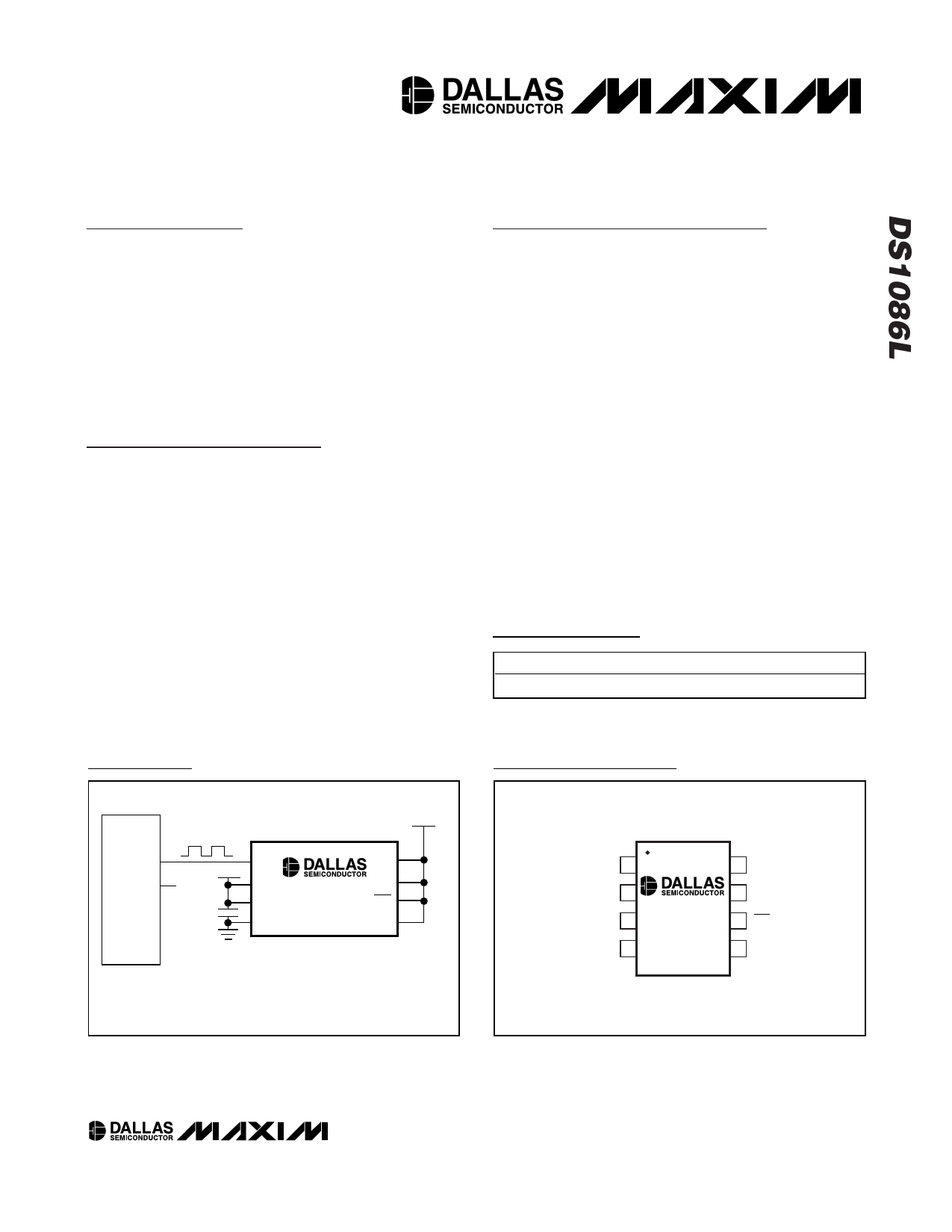
Typical Operating Circuit
DITHERED 130kHz TO
µP 66.6MHz OUTPUT
VCC
XTL1/OSC1
XTL2/OSC2
VCC OUT
N.C. SPRD
VCC
GND
DS1086L
SCL*
SDA*
PDN
OE
DECOUPLING CAPACITORS
(0.1µF and 0.01µF)
*SDA AND SCL CAN BE CONNECTED DIRECTLY HIGH IF THE DS1086L NEVER NEEDS
TO BE PROGRAMMED IN-CIRCUIT, INCLUDING DURING PRODUCTION TESTING.
TOP VIEW
Pin Configuration
OUT 1
SPRD 2
VCC 3
GND 4
DS1086L
8 SCL
7 SDA
6 PDN
5 OE
µSOP
EconOscillator is a trademark of Dallas Semiconductor.
______________________________________________ Maxim Integrated Products 1
For pricing, delivery, and ordering information, please contact Maxim/Dallas Direct! at
1-888-629-4642, or visit Maxim’s website at www.maxim-ic.com.
1 page 
3.3V Spread-Spectrum EconOscillator
AC ELECTRICAL CHARACTERISTICS—2-WIRE INTERFACE (continued)
(VCC = 2.7V to 3.6V, TA = -40°C to +85°C.)
PARAMETER
Setup Time for STOP
Capacitive Load for Each Bus
Line
EEPROM Write Cycle Time
Input Capacitance
SYMBOL
tSU:STO
CONDITIONS
Fast mode
Standard mode
CB (Note 16)
tWR
CI
MIN TYP
0.6
4.0
5
MAX
400
10
UNITS
µs
pF
ms
pF
NONVOLATILE MEMORY CHARACTERISTICS
(VCC = 2.7V to 3.6V)
PARAMETER
EEPROM Writes
SYMBOL
+70°C
CONDITIONS
MIN TYP
10,000
MAX UNITS
Note 1:
Note 2:
Note 3:
Note 4:
Note 5:
Note 6:
Note 7:
Note 8:
Note 9:
Note 10:
Note 11:
Note 12:
Note 13:
Note 14:
Note 15:
Note 16:
Note 17:
Note 18:
All voltages are referenced to ground.
DAC and OFFSET register settings must be configured to maintain the master oscillator frequency within this range.
Correct operation of the device is not guaranteed if these limits are exceeded.
This is the absolute accuracy of the master oscillator frequency at the default settings.
This is the change that is observed in master oscillator frequency with changes in voltage from nominal voltage at
TA = +25°C.
This is the percentage frequency change from the +25°C frequency due to temperature at VCC = 3.3V. The maximum temper-
ature change varies with the master oscillator frequency setting. The minimum occurs at the default master oscillator frequen-
cy (fdefault). The maximum occurs at the extremes of the master oscillator frequency range (33.3MHz or 66.6MHz).
The dither deviation of the master oscillator frequency is unidirectional and lower than the undithered frequency.
The integral nonlinearity of the frequency is a measure of the deviation from a straight line drawn between the two end-
points (fosc(MIN) to fosc(MAX)) of the range. The error is in percentage of the span.
This is true when the prescaler = 1.
Frequency settles faster for small changes in value. During a change, the frequency transitions smoothly from the original
value to the new value.
This indicates the time elapsed between power-up and the output becoming active. An on-chip delay is intentionally
introduced to allow the oscillator to stabilize. tstab is equivalent to approximately 512 master clock cycles and therefore
depends on the programmed clock frequency.
Output voltage swings can be impaired at high frequencies combined with high output loading.
A fast-mode device can be used in a standard-mode system, but the requirement tSU:DAT > 250ns must then be met.
This is automatically the case if the device does not stretch the LOW period of the SCL signal. If such a device does
stretch the LOW period of the SCL signal, it must output the next data bit to the SDA line at least tR MAX + tSU:DAT =
1000ns + 250ns = 1250ns before the SCL line is released.
After this period, the first clock pulse is generated.
A device must internally provide a hold time of at least 300ns for the SDA signal (referred to as the VIH MIN of the SCL
signal) to bridge the undefined region of the falling edge of SCL.
The maximum tHD:DAT need only be met if the device does not stretch the LOW period (tLOW) of the SCL signal.
CB—total capacitance of one bus line, timing referenced to 0.9 x VCC and 0.1 x VCC.
Typical frequency shift due to aging is ±0.5%. Aging stressing includes Level 1 moisture reflow preconditioning (24hr
+125°C bake, 168hr 85°C/85%RH moisture soak, and three solder reflow passes +240 +0/-5°C peak) followed by 1000hr
max VCC biased 125°C HTOL, 1000 temperature cycles at -55°C to +125°C, 96hr 130°C/85%RH/3.6V HAST and 168hr
121°C/2 ATM Steam/Unbiased Autoclave.
tstab is the time required after exiting power-down to the beginning of output oscillations. In addition, a delay of tDACstab
is required before the frequency will be within its specified tolerance.
_____________________________________________________________________ 5
5 Page 
3.3V Spread-Spectrum EconOscillator
JS2 to JS0: Jitter Percentage. These three bits select
the amount of jitter in percent. The SPRD pin must be a
logic high for the jitter to be enabled. Bit combinations
not shown are reserved.
JS2 JS1 JS0 JITTER %
0 0 0 0.5
001
1
010
2
100
4
111
8
Lo/HiZ: Output Low or High-Z. This bit determines the
state of the output pin when the device is in power-
down mode or when the output is disabled. If Lo/HiZ =
0, the output is HiZ when in power-down or disabled. If
Lo/HiZ = 1, the output is held low when in power-down
or disabled.
P3 to P0: Prescaler Divider. These bits divide the
master oscillator frequency by 2x, where x is P3 to P0
and can be from 0 to 8. Any prescaler value entered
greater than 8 decodes as 8.
DAC (08h)
B9 to B0: DAC Setting. The DAC word sets the master
oscillator frequency to a specific value within the cur-
rent offset range. Each step of the DAC changes the
master oscillator frequency by 5kHz. The DAC word is
read and written using two-byte reads and writes
beginning at address 08h.
OFFSET (0Eh)
B4 to B0: Offset. This value selects the master oscilla-
tor frequency range that can be generated by varying
the DAC word. Valid frequency ranges are shown in
Table 2. Correct operation of the device is not guaran-
teed for values of OFFSET not shown in the table.
The default offset value (OS) is factory trimmed and
can vary from device to device. Therefore, to change
frequency range, OS must be read so the new offset
value can be calculated relative to the default. For
example, to generate a master oscillator frequency
within the largest range (61.4MHz to 66.6MHz), Table 2
indicates that the OFFSET must be programmed to OS
+ 6. This is done by reading the RANGE register and
adding 6 to the value of bits B4 to B0. The result is then
written into bits B4 to B0 of the OFFSET register.
Additional examples are provided in the Example
Frequency Calculations section.
RANGE (37h)
B4 to B0: Range: This read-only, factory programmed
value is a copy of the factory default offset (OS). OS is
required to program new master oscillator frequencies
shown in Table 2. The read-only backup is important
because the offset register is EEPROM and is likely to
be overwritten.
ADDR (0Dh)
WC: EEPROM Write Control Bit. The WC bit
enables/disables the automatic writing of registers to
EEPROM. This prevents EEPROM wear out and elimi-
nates the EEPROM write cycle time. If WC = 0 (default),
register writes are automatically written to EEPROM. If
WC = 1, register writes are stored in SRAM and only
written into EEPROM when the user sends a WRITE EE
command. If power is cycled to the device, then the
last value stored in EEPROM is recalled. WC = 1 is
ideal for applications that frequently modify the fre-
quency/registers.
Regardless of the value of the WC bit, the value of the
ADDR register is always written immediately to EEPROM.
A2 to A0: Device Address Bits. These bits determine
the 2-wire slave address of the device. They allow up to
eight devices to be attached to the same 2-wire bus
and to be addressed individually.
WRITE EE Command (3Fh)
This command can be used when WC = 1 (see the WC
bit in ADDR register) to transfer all registers from SRAM
into EEPROM. The time required to store the values is
one EEPROM write cycle time. This command is not
needed if WC = 0.
____________________________________________________________________ 11
11 Page | ||
| Páginas | Total 16 Páginas | |
| PDF Descargar | [ Datasheet DS1086L.PDF ] | |
Hoja de datos destacado
| Número de pieza | Descripción | Fabricantes |
| DS1086 | Spread-Spectrum EconOscillator | Dallas Semiconductor |
| DS1086 | Spread-Spectrum EconOscillator | Maxim Integrated |
| DS1086L | Spread-Spectrum EconOscillator | Dallas Semiconductor |
| Número de pieza | Descripción | Fabricantes |
| SLA6805M | High Voltage 3 phase Motor Driver IC. |
Sanken |
| SDC1742 | 12- and 14-Bit Hybrid Synchro / Resolver-to-Digital Converters. |
Analog Devices |
|
DataSheet.es es una pagina web que funciona como un repositorio de manuales o hoja de datos de muchos de los productos más populares, |
| DataSheet.es | 2020 | Privacy Policy | Contacto | Buscar |